

Page 1
R
REDUCED HEIGHT MICRO-POWER CURRENT MONITOR
Description
The ZXCT1012 is a high side current sense monitor. Using
this type of device eliminates the need to disrupt the ground
plane when sensing a load current.
The ZXCT1012 takes the voltage developed across a small
value resistor and translates it into a proportional output
current. A user defined output resistor scales the output
current into a ground referenced voltage.
The ZXCT1012 has the accuracy specification of the
ZXCT1010 but in TSOT25.
A minimum operating current of just 3.5μA, combined with its
TSOT25 package make it suitable for portable battery
equipment where size and current consumption are critical.
The wide input voltage range down to as low as 2.5V make it
suitable for a wide range of applications requiring direct
operation from a battery.
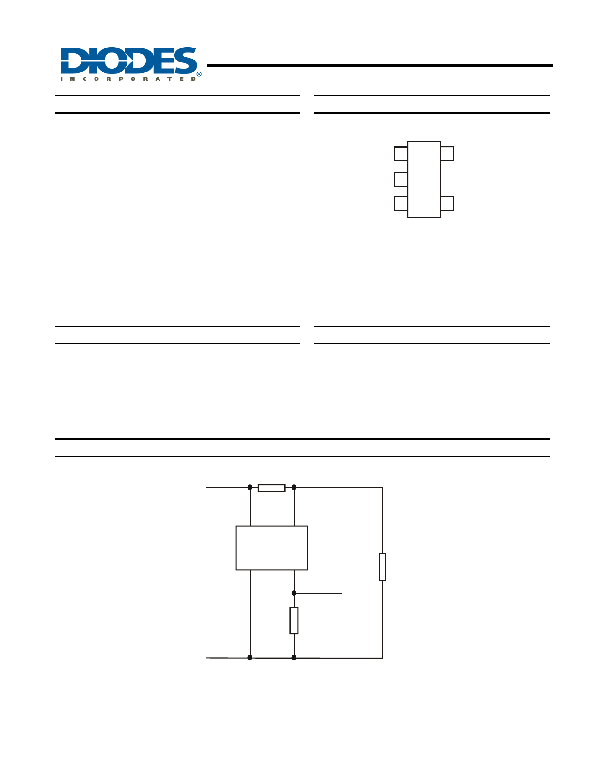
Pin Assignments
(Top View)
1
NC
GND
2
OUT
TSOT25
ZXCT1012
SENSE-
5
43
SENSE+
Features
• 2.5V to 20V supply range
• 3.5μA quiescent current
• Current output - user set gain
• Thin package - TSOT25
• Temperature range -40 to 85°C
Typical Application Circuit
V
Applications
• Battery fuel gauge
• Battery chargers
• Overcurrent monitor
• Power management
IN
SENSE
SENSE+ SENSE-
ZXCT1012
GND
OUT
R
LOAD
V
OUT
R
OUT
ZXCT1012
Document number: DS33444 Rev. 2 - 2
1 of 9
www.diodes.com
September 2011
© Diodes Incorporated
Page 2
ZXCT1012
Pin Descriptions
Pin Name Description
1 N/C
2 GND
3 OUT
4 SENSE+
5 SENSE-
Absolute Maximum Ratings (T
V
Voltage on any pin(relative to GND pin) -0.6 and V
V
Ambient Operating Temperature Range -40 to 85 °C
Storage Temperature -55 to 150 °C
Maximum Junction Temperature 150 °C
Power Dissipation (TA = 25°C)
Max. 20 V
SENSE+
(Note 1) -0.15 to 3 V
SENSE
Package
(Note 2)
TSOT25 250°C/W 500mW
Recommended Operating Conditions
Symbol Parameter Min. Max. Units
VIN Sense+ range 2.5 20 V
TA Ambient temperature range differential -40 85 C
V
Sense voltage 10 2500 mV
SENSE
V
Output voltage swing 0 V
OUT
Operation above the absolute maximum rating may cause device failure.
Operation at the absolute maximum ratings, for extended periods, may reduce device reliability.
Notes: 1. V
2. Mounted on 30mm x 16mm x1.1mm FR4 board with 1oz copper.
is defined as the differential voltage between the SENSE+ and SENSE- pins. (V
SENSE
ZXCT1012
Document number: DS33444 Rev. 2 - 2
No connection
Ground connection
Output current pin. Current generated due to a difference voltage
between V
value resistor connected to ground creates an output voltage. The
maximum voltage out of this pin will be V
This pin should be connected to the rail whose current is being
measured and also provides power to internal circuitry. It is the
positive input of the current monitor and has an input range from
20V down to 2.5V. The current through this pin varies with
differential sense voltage.
This is the negative input of the current monitor and has an input
range from 20V down to 2.5V.
Description Rating Unit
R
P
θJA
REDUCED HEIGHT MICRO-POWER CURRENT MONITOR
SENSE+
and V
= 25°C)
A
@ 25°C
DISS
flows out of this pin. A suitable
SENSE-
SENSE-
300
(De-rate to 0 at 150°C)
2 of 9
www.diodes.com
- 1.5V.
+0.5 V
SENSE+
mW
-15 V
SENSE-
SENSE
= V
SENSE+
- V
SENSE-
)
September 2011
© Diodes Incorporated
Page 3
ZXCT1012
Electrical Characteristics (T
Symbol Parameter Conditions
I
Output Current
OUT
IQ Ground Pin Current V
I
SENSE- Pin Input Current 100 nA
SENSE-
ACC Accuracy
Gm
TC Temperature Coefficient
BW Bandwidth
CMRR
(Note 4)
Notes: 3. Temperature dependent measurements are extracted from characterisation and simulation results.
4. With the ZXCT1012 using SENSE+ as its power supply pin, common mode rejection cannot be distinguished from power supply rejection.
Transconductance,I
(Note 3)
Common Mode Rejection Ratio
ZXCT1012
Document number: DS33444 Rev. 2 - 2
OUT/VSENSE
REDUCED HEIGHT MICRO-POWER CURRENT MONITOR
= 25°C, VIN = V
A
V
SENSE
V
SENSE
V
SENSE
V
SENSE
V
SENSE
SENSE
R
SENSE
V
SENSE
V
SENSE
TA = 0 to 50°C (Note 3)
= 5pF
C
L
R
OUT
V
SENSE
VIN = 2.5V to 20V
SENSE+
= 0V
= 10mV
= 40mV
= 100mV
= 200mV
= 0V 3.5 8 µA
= 0.1V
= 200mV
= 200mV
= 1kΩ
= 100mV, R
= 5V; unless otherwise specified)
Limits
Min. Typ. Max.
V
SENSE
V
SENSE
= 10mV
= 100mV
= 1kΩ
OUT
0
85
380
0.975
1.95
-2.5 2.5 %
10 mA/V
500 ppm/°C
80 dB
0.3
100
400
1.00
2.00
300
2
15
115
420
1.025
2.05
3 of 9
www.diodes.com
September 2011
© Diodes Incorporated
Unit
µA
µA
µA
mA
mA
kHz
MHz
Page 4

T
P
T
CURRENT
A
T
PUT CURRENT
A
G
A
d
OUT
P
U
T CUR
R
E
N
T (m
A
0
REJ
C
O
d
Typical Characteristics
ZXCT1012
REDUCED HEIGHT MICRO-POWER CURRENT MONITOR
10m
)
(
100µ
U
OUT
I, OU
)
(m
-2%
V = 5V
IN
T = 25°C
A
Ω
R = 0
OUT
1m
10µ
1µ
100µ 1m 10m 100m 1
V (V)
SENSE
Ty pical Output vs. Sense Voltag e
2%
0%
V = 5V
IN
V = 0.2V
SENSE
R = 0
Ω
OUT
4
V = 5V
IN
T = 25°C
A
R = 0
Ω
3
OUT
2
Typical
1
0
OUTPUT CURRENT ERROR (%)
-1
1m 10m 100m 1
3
V = 5V
IN
°
T = 25C
A
V = 63.2mVpp
SENSE(AC)
V (V)
SENSE
Error vs. S ense Voltage
0
DC V = 0.01V
-3
B)
IN (
SENSE
V = 0.1V
SENSE
-6
-4%
OUT
I, OU
-6%
12
10
)
OUT
I,
-40
V = 5V
T = 25C
R = 0
8
6
4
2
-20 0 20 40 60 80
TEMPERATURE (°C)
Output Cur r ent vs. Temperature
IN
°
A
OUT
Ω
V = 1V
SENSE
V = 0.8V
SENSE
V = 0.6V
SENSE
V = 0.4V
SENSE
V = 0.2V
SENSE
-9
-12
0.01 0.1 1 10
FREQUENCY (MHz)
Frequency Response
V = 5V
IN
°
T = 25C
A
-10
V = 63.2Vpp
SENSE(AC)
-20
-30
B)
N (
-40
TI
-50
E
V = 0.01V
SENSE
-60
-70
V = 1V
SENSE
V = 0.1V
SENSE
V = 1V
SENSE
-80
0
102345
V , SUPPLY VOLTAGE (V)
IN
Tran sf er Characteristics
ZXCT1012
Document number: DS33444 Rev. 2 - 2
4 of 9
www.diodes.com
-90
1 10 100 1k 10k
FREQUENCY (Hz)
Common Mode Rejection
100k 1M 10M
September 2011
© Diodes Incorporated
Page 5

ZXCT1012
Applications Information
The ZXCT1012 current monitor works by converting the voltage deve lope d across a sma ll se nse res istor into a c urrent on the
out pin. In reality it is a voltage to current converter. This output current can be converted into a volta ge simply by passing it
through a resistor (R
The current monitor has a transconductance of 10mA/V. But the overall amplifying conversion is affected by both the R
OUT
.
and R
The gain equation of the ZXCT1012 is:
) to ground.
OUT
REDUCED HEIGHT MICRO-POWER CURRENT MONITOR
SENSE
R
OUT
I
SENSE
L
V ×=
R
OUT
100
For best performance R
resistance with R
SENSE
When choosing appropriate values for R
should be connected as close to the SENSE+ (and SENSE-) pins; which minimizes any series
SENSE
and potential for interference pickup.
a compromise must be reached between in-line sign al loss (including p otential
SENSE
power dissipation effects) and small signal accuracy.
Higher values for R
best operation the ZXCT1012 has been designed to provide best performance with V
gives better accuracy at low load currents by reducing the inaccuracies due to internal offsets. For
SENSE
of the order of 40mV to 200mV.
SENSE
Current monitors are single supply devices which means they tend to saturate at ver y low sense voltages. However it does
mean the output can never go negative. Also the output can never change direction (monotonic). This is important if the
current monitor is used in a control loop.
As the sense voltage is reduced the output will tend to saturate as the input offset voltage starts to have greater effect. It is
recommended to have a minimum sense voltage of 10mV to minimize linearity errors. Diodes has specified the output voltage
at V
The maximum differential input voltage, V
of 10mV, 40mV, 100mV and 200mV; which is the recommended sense voltage range.
SENSE
, is 2.5V; however this will cause large output currents to flow increasing power
SENSE
dissipation in the chip. The sense voltage can be increased further, without damaging the ZXCT1012, by the inclus ion of a
resistor, R
, between SENSE- pin and the load. Typical values around 10kΩ. See figure below.
LIM
R
SENSE
R
C
C
LIM
ZXCT1012
If large reverse currents are expected then the resistor, R
A suitable value for R
Where V
SENSE(REV)
ZXCT1012
Document number: DS33444 Rev. 2 - 2
can be determined from:
LIM
R
LIM
is the maximum expected reverse sense voltage generated.
www.diodes.com
, will provide protection from exceeding absolute maximum ratings.
LIM
V
=
)REF(SENSE
mA5
5 of 9
September 2011
© Diodes Incorporated
Page 6

R
REDUCED HEIGHT MICRO-POWER CURRENT MONITOR
Applications Information
(cont.)
The following lines describe how to scale a load current to an output voltage.
V
= R
SENSE
I
= 10mA/V x V
OUT
V
= I
OUT
Design example
In the circuit below a 1A current is to be represented by a 100mV output voltage (V
A) To be within recommended values choose the value of R
50mV > V
For example set V
From equation (1)
R
SENSE
B) Now choose R
V
OUT
From equation (2)
I
OUT
Rearranging equation (3) for R
R
OUT
V
IN
SENSE
= 0.1V/1.0A = 0.1Ω
= 100mV, when V
= 10mA/V x 0.1 = 1mA
= V
OUT/IOUT
* I
SENSE
OUT
x R
equation (1)
LOAD
equation (2)
SENSE
equation (3)
OUT
> 200mV at full load.
= 100mV at 1.0A.
SENSE
to give:
OUT
= 100mV.
SENSE
gives:
OUT
= 0.1/0.001 = 100Ω
SENSE
SENSE
to give:
OUT
ZXCT1012
):
SENSE+ SENSE-
ZXCT1012
GND
OUT
R
LOAD
V
OUT
R
OUT
= 0.1 / (0.1 x 0.01) = 100Ω
Typical Circuit Application
Where R
represents any load including DC motors, a charging battery or further circuitry that requires monitoring, R
LOAD
can be selected on specific requirements of accuracy, size and power rating.
ZXCT1012
Document number: DS33444 Rev. 2 - 2
6 of 9
www.diodes.com
September 2011
© Diodes Incorporated
SENSE
Page 7

ZXCT1012
) watts
), maximum junction temperature (T
JA
Power Dissipation
The maximum allowable power dissipation of the device for normal operation (P
ambient thermal resistance (θ
expression:
= (T
P
MAX
The device power dissipation, PD is given by the expression:
PD = I
OUT
Care must be taken when using this device at large input voltages and large sense voltages to prevent too much power
dissipation.
600
500
400
– TA) / θJA
JMAX
.(VIN-V
OUT
REDUCED HEIGHT MICRO-POWER CURRENT MONITOR
), is a function of the package junction to
MAX
), and ambient temperature (TA), according to the
JMAX
300
200
100
0
0 255075100125150
T , AMBIENT TEMPERATURE ( C)
A
VIN = 20V V
= 100Ω
R
OUT
I
= 2.5 x 0.01
OUT
= 25mA
= I
V
OUT
OUT
= 25mA x 100Ω
= 2.5V
P
= 25mA (20 - 2.5)V
D
= 438mW
x R
SENSE
OUT
= 2.5V
ZXCT1012
Document number: DS33444 Rev. 2 - 2
°
7 of 9
www.diodes.com
September 2011
© Diodes Incorporated
Page 8

ZXCT1012
θ
Ordering Information
Device Package Marking Reel Size Quantity
ZXCT1012ET5TA TSOT25 1012 7 3000 Tape & Reel
Package Outline Dimensions (All Dimensions in mm)
D
E1
A2
A
A1
Suggested Pad Layout
ZXCT1012
Document number: DS33444 Rev. 2 - 2
e1
e
5x b
Y1
REDUCED HEIGHT MICRO-POWER CURRENT MONITOR
E
C C
4x 1
θ
Y (5x)
X (5x)
www.diodes.com
c
L
8 of 9
L2
Dimensions Value (in mm)
C
X
Y
Y1
TSOT25
Dim Min Max Typ
A
A1 0.01 0.10
A2 0.84 0.90
D
E
E1
b 0.30 0.45
c 0.12 0.20
e
e1
L 0.30 0.50
L2
θ 0° 8° 4°
θ1 4° 12°
All Dimensions in mm
1.00
−
− −
− −
− −
− −
− −
− −
0.950
0.700
1.000
3.199
−
−
−
2.90
2.80
1.60
−
−
0.95
1.90
0.25
−
September 2011
© Diodes Incorporated
Page 9

ZXCT1012
DIODES INCORPORATED MAKES NO WARRANTY OF ANY KIND, EXPRESS OR IMPLIED, WITH REGARDS TO THIS
DOCUMENT, INCLUDING, BUT NOT LIMITED TO, THE IMPLIED WARRANTIES OF MERCHANTABILITY A ND FITNESS FOR A
PARTICULAR PURPOSE (AND THEIR EQUIVALENTS UNDER THE LAWS OF ANY JURISDICTION).
Diodes Incorporated and its subsidiaries reserve the right to make modifications, enhancements, improvements, corrections or other
changes without further notice to this document and any product described herein. Diodes Incorporat ed does not assume any liability
arising out of the application or use of this document or any product described herein; neither does Diodes Incorporated convey any
license under its patent or trademark rights, nor the rights of others. A ny Customer or user of this document or products described
herein in such applications shall assume all risks of such use and will agree to hold Diodes Incorporated and all the companies
whose products are represented on Diodes Incorporated website, harml ess ag ai nst all damages.
Diodes Incorporated does not warrant or acc ept any liability whatsoever in respec t of any products purchas ed through unauthorized
sales channel.
Should Customers purchase or use Diodes Incorporated products for any unintended or unauthorized application, Customers shall
indemnify and hold Diodes Incorporated and its representatives harmless agai nst all claims, damages, expenses, and attorney fees
arising out of, directly or indirectly, any claim of personal injury or death ass ociated with such unintended or unauthorized application.
Products described herein may be covered by one or more United Stat es, international or foreign patents pending. Product names
and markings noted herein may also be covered by one or more United States, international or foreign trademarks.
Diodes Incorporated products are specifically not authorized for use as critical components in life support devices or systems without
the express written approval of the Chief Executive Officer of Diodes Incorporated. As used herei n:
A. Life support devices or systems are devices or systems which:
1. are intended to implant into the body, or
2. support or sustain life and whose failure to perform when properly used in accordance with instructi ons for us e provided
in the labeling can be reasonably expected to result in significant injury to the user.
B. A critical component is any component in a life support device or system whose failure t o perform can be reasonably expected
to cause the failure of the life support device or to affect its safety or effectiveness .
Customers represent that they have all necessary expertise in the safety and regulatory ramifications of their life support devices or
systems, and acknowledge and agree that they are solely responsible for all legal, regulatory and safety-related requirements
concerning their products and any use of Diodes Incorporated products in such safety-critical, life support devices or systems,
notwithstanding any devices- or systems-related information or support that may be provided by Diodes Incorporated. Further,
Customers must fully indemnify Diodes Incorporated and its representatives agai nst any damages arising out of the use of Diodes
Incorporated products in such safety-critic al, l ife support devic es or syst ems .
Copyright © 2011, Diodes Incorporated
www.diodes.com
REDUCED HEIGHT MICRO-POWER CURRENT MONITOR
IMPORTANT NOTICE
LIFE SUPPORT
ZXCT1012
Document number: DS33444 Rev. 2 - 2
9 of 9
www.diodes.com
September 2011
© Diodes Incorporated
 Loading...