

Page 1
SEMICONDUCTORS
ENHANCED HIGH-SIDE CURRENT MONITOR
ZXCT1010
DESCRIPTION
The ZXCT1010 is a high side current sense monitor.
Using this device eliminates the need to disrupt the
ground plane when sensing a load current.
It is an enhanced version of the ZXCT1009 offering
reduced typical output offset and improved accuracy
at low sense voltage.
The wide inputvoltage range of 20V downto aslow as
2.5V make it suitable for a range of applications. A
minimum operating current of just 4µA, combined
with its SOT23-5 package make suitable for portable
battery equipment.
FEATURES
• Low cost, accurate high-side current sensing
• Output voltage scaling
• Up to 2.5V sense voltage
• 2.5V – 20V supply range
• 300nA typical offset current
• 3.5µA quiescent current
• 1% typical accuracy
•
SOT23 -5 package
APPLICATIONS
Battery chargers
•
Smart battery packs
•
DC motor control
•
Over current monitor
•
Power management
•
Programmable current source
•
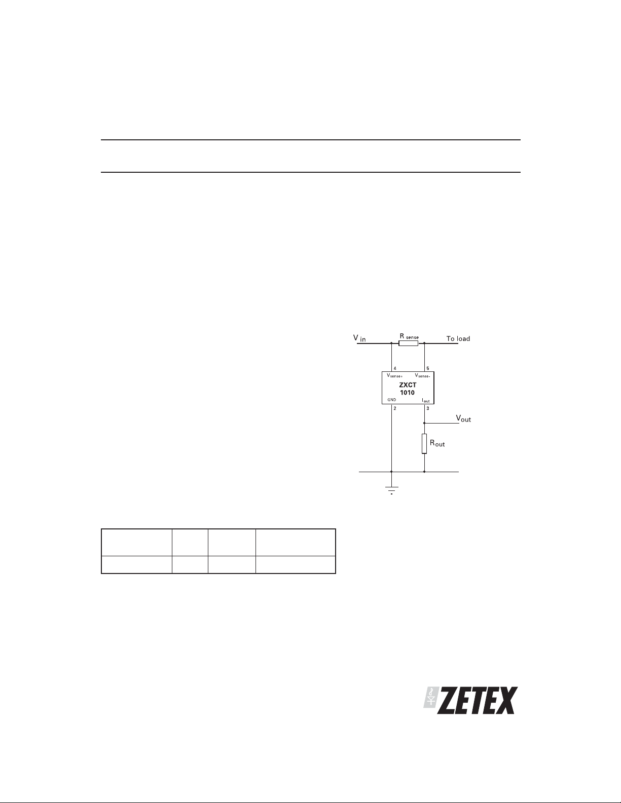
APPLICATION CIRCUIT
ORDERING INFORMATION
DEVICE REEL
ZXCT1010E5TA 7” 8mm 3,000 units
PARTMARK 101
PACKAGE SOT23-5
ISSUE 10 - JULY 2007
SIZE
TAPE
WIDTH
QUANTITY PER
REEL
1
Page 2
SEMICONDUCTORS
ZXCT1010
ABSOLUTE MAXIMUM RATINGS
Voltage on any pin -0.6V to 20V (relative to GND)
Continuous output current, I
Continuous sense voltage, V
Operating temperature, T
Storage temperature -55 to 150°C
Package power dissipation (T
SOT23-5 300mW
Operation above the absolute maximum rating may cause device failure.
Operation at the absolute maximum ratings, for extended periods, may reduce device reliability.
ELECTRICAL CHARACTERISTICS
Test Conditions TA= 25°C, Vin= 5V, R
SYMBOL PARAMETER CONDITIONS LIMITS UNIT
V
in
I
out
I
q
V
sense
I
sense
Acc Accuracy
Gm Transconducta
BW Bandwidth V
1
Includes input offset voltage contribution
2
V
SENSE
3
-20dBm=63mVp-p into 50Ω
VCCRange 2.5 20 V
1
Output current V
Ground pin
current
2
Sense Voltage 0 2500 mV
-V
sense
-
input current
nce,
I
out/Vsense
is defined as the differential voltage between V
V
= V
SENSE
SENSE+
= VIN- V
= I
LOAD
LOAD
x R
,
A
- V
SENSE
OUT
SENSE-
, 25mA
2
, -0.5V to +5V
SENSE
sense
V
sense
V
sense
V
sense
V
sense
V
sense
R
sense
V
sense
SENSE(DC)
V
SENSE(DC)
-40 to 85°C
= 25°C)
A
= 100Ω.
out
Min Typ Max
=0V
= 10mV
=100mV
= 200mV
=1V
0
85
0.975
1.95
9.7
0.3
100
1.00
2.00
10.0
10
115
1.025
2.05
10.3
=0V 3.5 8 µA
100 nA
=0.1Ω
=200mV
-2.5 2.5 %
10000 µA/V
= 10mV, Pin = -40dBm ‡
= 100mV, Pin = -20dBm ‡
and V
SENSE+
SENSE-
.
300
2
µA
µA
mA
mA
mA
kHz
MHz
ISSUE 10 - JULY 2007
Page 3
SEMICONDUCTORS
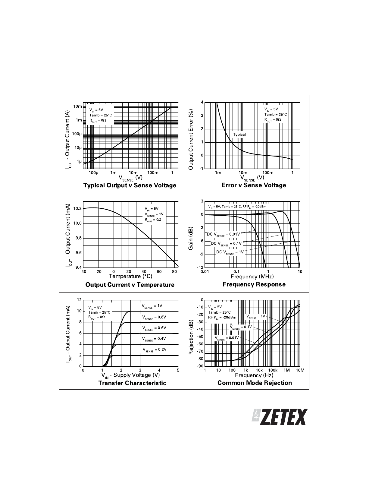
TYPICAL CHARACTERISTICS
ZXCT1010
ISSUE 10 - JULY 2007
3
Page 4

SEMICONDUCTORS
ZXCT1010
PIN DESCRIPTION
Pin Name Pin Function
+ Supply voltage
V
sense
V
- Connection to load/battery
sense
I
out
GND Ground
CONNECTION DIAGRAM
SOT23-5
Package Suffix – E5
Top View
Output current, proportional to Vin-V
load
SCHEMATIC DIAGRAM
ISSUE 10 - JULY 2007
4
Page 5

SEMICONDUCTORS
ZXCT1010
POWER DISSIPATION
The maximum allowable power dissipation of the
device for normal operation (Pmax), is a function of
the package junction to ambient thermal resistance
(θja), maximum junction temperature (Tjmax), and
ambient temperature (Tamb), according to the
expression:
P
max
= (Tj
max
– T
amb
) / θ
ja
The device power dissipation, PDis given by the
expression:
P
D=Iout
.(Vin-V
) Watts
out
APPLICATIONS INFORMATION
The following lines describe how to scale a load
current to an output voltage.
= Vin-V
V
V
out
sense
= 0.01 x V
sense
load
x R
out
1
E.g.
A 1A current is to be represented by a 100mV output
voltage:
1)Choose the value of R
to give 50mV > V
sense
sense
500mV at full load.
For example V
= 100mV at 1.0A. R
sense
sense
= 0.1/1.0
=> 0.1 ohms.
2)Choose R
to give V
out
= 100mV, when V
out
sense
100mV.
/(V
1
for R
sense
gives:
out
x 0.01)
Rearranging
R
out=Vout
= 0.1 / (0.1 x 0.01) = 100 Ω
R
out
TYPICAL CIRCUIT APPLICATION
>
=
ISSUE 10 - JULY 2007
Where R
represents any load including DC motors,
load
a charging battery or further circuitry that requires
monitoring, R
canbeselectedonspecific
sense
requirements of accuracy, size and power rating.
5
Page 6

SEMICONDUCTORS
ZXCT1010
100Ω
0.2Ω
100Ω
FZT789A
BC81725
1kΩ
BAS16
10µH
FMMT451
140µH
ZHCS1000
220Ω
SNS pin
MOD pin
Charger Input To Battery +
bq2954
5V
ZXCT1010
support components omitted for clarity
+
-
V
in
Load
I
out
-400 -200 0 200 400
0
1
2
3
4
5
Output Current (mA)
Sense Voltage (mV)
Output Current v Sense Voltage
APPLICATIONS INFORMATION (Continued)
Li-Ion Charger Circuit
The above figure shows the ZXCT1010 supporting
the Benchmarq bq2954 Charge Management IC.
Most of the support components for the bq2954 are
omitted for clarity. This design also uses the Zetex
FZT789A high current Super- PNP as the switching
transistor in the DC-DC step down converter and the
FMMT451 as the drive NPN for the FZT789A. The
circuit can be configured to charge up to four Li-Ion
cells at a charge current of 1.25A. Charge can be
terminated on maximum voltage, selectable
minimum current, or maximum time out. Switching
frequency of the PWM loop is approximately 120kHz.
Bi-Directional Current Sensing
The ZXCT1010 can be used to measure current
bi-directionally, if two devices are connected as
shown below.
If the voltage V1 is positive with respect to the
voltage V2 the lower device will be active, delivering
a proportional output current to Rout. Due to the
polarity of the voltage across Rsense, the upper
device will be inactive and will not contribute to the
current delivered to Rout. When V2 is more positive
than V1, current will be flowing in the opposite
direction, causing the upper device to be active
instead.
Non-linearity will be apparent at small values of
Vsense due to offset current contribution. Devices
can use separate output resistors if the current
direction is to be monitored independently.
Bi-directional Transfer Function
ISSUE 10 - JULY 2007
6
Page 7

SEMICONDUCTORS
APPLICATIONS INFORMATION (Continued)
PCB trace shunt resistor for low cost
solution
The figure below shows output characteristics of the
device when usinga PCB resistivetrace for a low cost
solution in replacement for a conventional shunt
resistor. The graph shows the linear rise in voltage
across the resistor due to the PTC of the material and
demonstrates how this rise in resistance value over
temperature compensates forthe NTC ofthe device.
The figureopposite shows a PCB layout suggestion.
The resistor section is 25mm x 0.25mm giving
approximately 150mΩ using 1oz copper. The data
for the normalised graph was obtained using a 1A
load current and a 100Ω output resistor. An
electronic version of the PCB layout is available at
www.zetex.com/isense
ZXCT1010
Actual Size
Layout shows area of shunt
resistor compared to SOT23-5
package. Not actual size
ISSUE 10 - JULY 2007
7
Page 8

SEMICONDUCTORS
ZXCT1010
Definitions
Product change
Zetex Semiconductors reserves the right to alter, without notice, specifications, design, price or conditions of supply of any product or service.
Customers are solely responsible for obtaining the latest relevant information before placing orders.
Applications disclaimer
The circuitsin this design/application note areoffered as design ideas. Itis the responsibility ofthe user to ensure thatthe circuit is fit forthe user's
application andmeets with theuser's requirements. Norepresentation or warranty is givenand no liabilitywhatsoever is assumedby Zetex with
respect to the accuracy or use of such information, or infringement of patents or other intellectual property rights arising from such use or
otherwise. Zetex does not assume any legal responsibility or will not be held legally liable (whether in contract, tort (including negligence),
breach ofstatutory duty, restriction or otherwise)for any damages,loss of profit,business, contract,opportunity or consequentialloss in the use
of these circuit applications, under any circumstances.
Life support
Zetex products are specifically not authorized for use as critical components in life support devices or systems without the express written
approval of the Chief Executive Officer of Zetex Semiconductors plc. As used herein:
A. Life support devices or systems are devices or systems which:
1. are intended to implant into the body
or
2. support or sustain life and whose failure to perform when properly used in accordance with instructions
for use provided in the labeling can be reasonably expected to result in significant injury to the user.
B. A critical component is any component in a life support device or system whose failure to perform can be reasonably expected to cause the
failure of the life support device or to affect its safety or effectiveness.
Reproduction
The product specifications contained in this publication are issued to provide outline information only which (unless agreed by the company in
writing) maynot be used, applied orreproduced forany purpose or form part of any orderor contract or be regardedas a representation relating
to the products or services concerned.
Terms and Conditions
All productsare sold subjects to Zetex'terms and conditions of sale,and this disclaimer (save in the eventof a conflictbetween thetwo when the
terms of the contract shall prevail) according to region, supplied at the time of order acknowledgement.
For the latest information on technology, delivery terms and conditions and prices, please contact your nearest Zetex sales office.
Quality of product
Zetex is an ISO 9001 and TS16949 certified semiconductor manufacturer.
To ensure quality of service and products we strongly advise the purchase of parts directly from Zetex Semiconductors or one of ourregionally
authorized distributors. For a complete listing of authorized distributors please visit: www.zetex.com/salesnetwork
Zetex Semiconductors does not warrant or accept any liability whatsoever in respect of any parts purchased through unauthorized sales
channels.
ESD (Electrostatic discharge)
Semiconductor devices are susceptible to damage by ESD. Suitable precautions should be taken when handling and transporting devices. The
possible damage to devices depends on the circumstances of the handling and transporting, and the nature of the device. The extent of damage
can vary from immediatefunctional orparametric malfunction to degradation offunction or performance in use over time.Devices suspectedof
being affected should be replaced.
Green compliance
Zetex Semiconductorsis committed toenvironmental excellencein all aspects of itsoperations which includes meeting orexceeding regulatory
requirements with respect to the use of hazardous substances. Numerous successful programs have been implemented to reduce the use of
hazardous substances and/or emissions.
All Zetex components are compliant with the RoHS directive, and through this it is supporting its customers in their compliance with WEEE and
ELV directives.
Product status key:
"Preview"Future device intended for production at some point. Samples may be available
"Active"Product status recommended for new designs
"Last time buy (LTB)"Device will be discontinued and last time buy period and delivery is in effect
"Not recommended for new designs"Device is still in production to support existing designs and production
"Obsolete"Production has been discontinued
Datasheet status key:
"Draft version"This term denotes a very early datasheet version and contains highly provisional
information, which may change in any manner without notice.
"Provisional version"This term denotes a pre-release datasheet. It provides a clear indication of anticipated performance. However, changes to
ISSUE 10 - JULY 2007
8
Page 9

ZXCT1010
SEMICONDUCTORS
PACKAGE DIMENSIONS
PAD LAYOUT DETAILS
Controlling dimensions are in millimeters. Approximate conversions are given in inches
PACKAGE DIMENSIONS
DIM Millimeters Inches DIM Millimeters Inches
MINMAXMINMAX MINMAXMINMAX
A 0.90 1.45 0.035 0.057 E 2.60 3.00 0.102 0.118
A1 0.00 0.15 0.00 0.006 E1 1.50 1.75 0.059 0.069
A2 0.90 1.3 0.035 0.051 e 0.95 REF 0.037 REF
b 0.35 0.50 0.014 0.020 e1 1.90 REF 0.075 REF
C 0.09 0.20 0.0035 0.008 L 0.10 0.60 0.004 0.024
D 2.80 3.00 0.110 0.118 a° 0 10 0 10
© Zetex Semiconductors plc 2007
Europe
Zetex GmbH
Kustermann-Park
Balanstraße 59
D-81541 München
Germany
Telefon: (49) 89 45 49 49 0
Fax: (49) 89 45 49 49 49
europe.sales@zetex.com
Americas
Zetex Inc
700 Veterans Memorial Hwy
Hauppauge, NY 11788
USA
Telephone: (1) 631 360 2222
Fax: (1) 631 360 8222
usa.sales@zetex.com
ISSUE 10 - JULY 2007
Asia Pacific
Zetex (Asia) Ltd
3701-04 Metroplaza Tower 1
Hing Fong Road, Kwai Fong
Hong Kong
Telephone: (852) 26100 611
Fax: (852) 24250 494
asia.sales@zetex.com
9
Corporate Headquarters
Zetex Semiconductors plc
Zetex Technology Park
Chadderton, Oldham, OL9 9LL
United Kingdom
Telephone (44) 161 622 4444
Fax: (44) 161 622 4446
hq@zetex.com
 Loading...