

Page 1
ZXCL SERIES
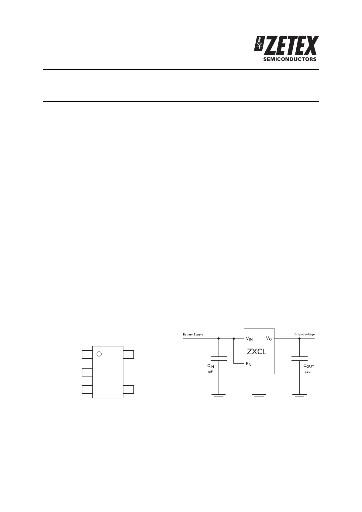
V
IN
GND
EN
V
O
NC
Top view
Micropower SC70-5 & SOT23-5 low dropout regulators
ZXCL5213V25, ZXCL5213V26, ZXCL5213V28, ZXCL5213V30, ZXCL5213V33, ZXCL250, ZXCL260, ZXCL280, ZXCL300, ZXCL330
Description
The ZXCL series have been designed with space
sensitive systems in mind. They are available in
the ultra small SC70-5 package, which is half the
size of SOT23 based regulators.
The devices can be used with all types of output
capacitors including low ESR ceramics and
typical dropout voltage, is only 85mV at 50mA
load. Supply current is minimised with a ground
pin current of only 50
Logic control allows the devices to be shut
down, consuming typically less than 10nA.
These features make the device ideal for battery
powered applications where power economy is
critical.
For applications requiring improved
performance over alternative devices, the
ZXCL is also offered in the 5 pin SOT23
package with an industry standard pinout.
The devices feature thermal overload and
over-current protection and are available with
output voltages of 2.5V, 2.6V, 2.8V, 3V, 3.3V.
A at full 150mA load.
Package footprint
SOT23-5 (see P7 for SC70-5)
Package suffix - E5
Features
• Low 85mV dropout at 50mA load
•50
A ground pin current with full 150mA load
• 2.5, 2.6, 2.8, 3, & 3.3 volts output
• Very low noise, without bypass capacitor
• 5-pin SC70 and SOT23 package
• No-load stable
Applications
• Cellular and Cordless phones
•PDA
• Hand held instruments
• Camera, Camcorder, Personal stereo
•PC cards
• Portable and battery-powered equipment
No-Load Stability
is stable with no external load. e.g. CMOS RAM applacations.
, the ZXCL device will maintain regulation and
Typical application circuit
Issue 8 - October 2007 1 www.zetex.com
© Zetex Semiconductors plc 2007
Page 2
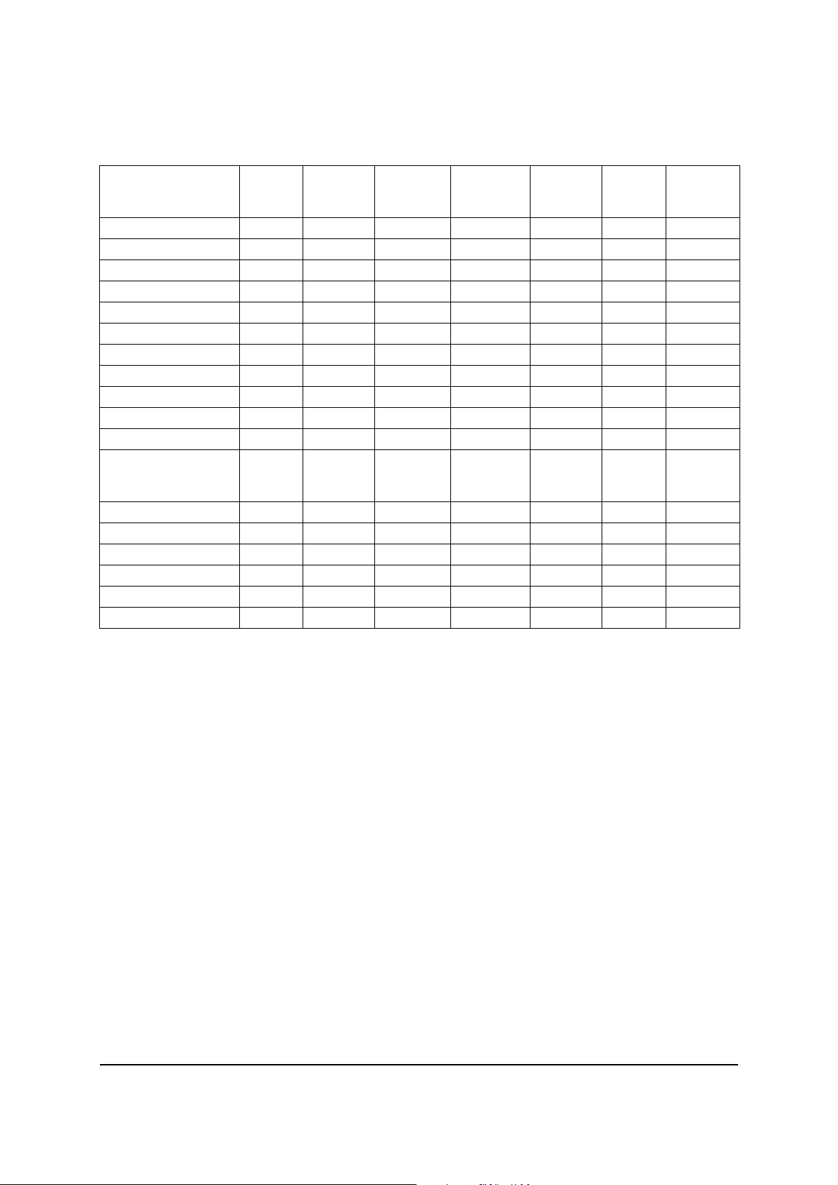
Ordering information
ZXCL SERIES
Order reference Voltage
(V)
ZXCL250H5TA 2.5 SC70-5 L25A Active 7 8 3000
ZXCL260H5TA 2.6 SC70-5 L26A Active 7 8 3000
ZXCL280H5TA 2.8 SC70-5 L28A Active 7 8 3000
ZXCL300H5TA 3.0 SC70-5 L30A Active 7 8 3000
ZXCL330H5TA 3.3 SC70-5 L33A Active 7 8 3000
ZXCL400H5TA 4.0 SC70-5 L40A Obsolete 7 8 3000
ZXCL5213V25H5TA 2.5 SC70-5 L25C Active 7 8 3000
ZXCL5213V26H5TA 2.6 SC70-5 L26C Active 7 8 3000
ZXCL5213V28H5TA 2.8 SC70-5 L28C Active 7 8 3000
ZXCL5213V30H5TA 3.0 SC70-5 L30C Active 7 8 3000
ZXCL5213V33H5TA 3.3 SC70-5 L33C Active 7 8 3000
ZXCL5213V40H5TA 4.0 SC70-5 L40C Not rec.
ZXCL250E5TA 2.5 SOT23-5 L25B Active 7 8 3000
ZXCL260E5TA 2.6 SOT23-5 L26B Active 7 8 3000
ZXCL280E5TA 2.8 SOT23-5 L28B Active 7 8 3000
ZXCL300E5TA 3.0 SOT23-5 L30B Active 7 8 3000
ZXCL330E5TA 3.3 SOT23-5 L33B Active 7 8 3000
ZXCL400E5TA 4.0 SOT23-5 L40B Obsolete 7 8 3000
Package Part
marking
Status Reel size
(inches)
7 8 3000
for new
designs
Tape
width
(mm)
Quantity
per reel
Absolute maximum rating
Terminal Voltage with respect to GND
V
IN
E
N
V
O
Package power dissipation (T
-0.3V to 7.0V
-0.3V to 10V
-0.3V to 5.5V
=25°C)
A
SC70-5 300mW (Note 1)
SOT23-5 450mW (Note 1)
Stresses beyond those listed under “Absolute maximum ratings” may cause permanent damage
to the device. These are stress ratings only, and functional operation of the device at these or any
other conditions beyond those indicated in the operational sections of the specifications is not
implied. Exposure to absolute maximum conditions for extended periods may affect device
reliability.
Output short circuit duration Infinite
Continuous power dissipation Internally limited
Operating temperature range -40°C to +85°C
Storage temperature range -55°C to +125°C
Issue 8 - October 2007 2 www.zetex.com
© Zetex Semiconductors plc 2007
Page 3
ZXCL SERIES
Recommended operating conditions
Symbol Parameter Min Max Units
V
IN
V
ENH
V
ENL
T
A
* Output voltage will start to rise when VIN exceeds a value or approximately 1.3V. For normal operation,
V
IN(min)
Input voltage range 2.0* 5.5 V
Enable pin logic level High pin 2.2 10 V
Enable pin logic level Low pin 0 0.8 V
Ambient temperature range -40 85 °C
> V
OUT(nom)
+ 0.5V.
Pin description
Symbol Parameter
V
IN
G
ND
E
N
N/C No connection
V
O
Supply voltage
Ground
Active HIGH enable input. TTL/CMOS logic compatible. Connect to V
or logic high for normal operation
Regulator output
IN
Issue 8 - October 2007 3 www.zetex.com
© Zetex Semiconductors plc 2007
Page 4
ZXCL SERIES
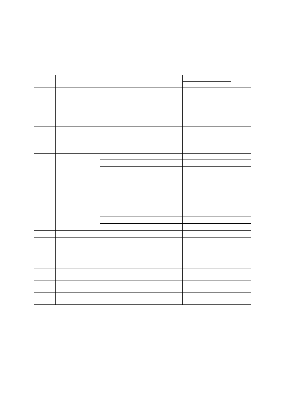
Electrical characteristics
VIN = VO = 0.5V, all values at TA = 25°C (Unless otherwise stated)
Symbol Parameter Conditions Limits Units
Min. Typ. Max.
V
O
⌬V
O
I
O(Max)
I
OLIM
I
O
V
DO
⌬V
LNR
⌬V
LDR
E
N
V
ENHS
I
EN
I
OSD
T
SD
Device testing is performed at TA=25°C. Device thermal performance is guaranteed by design.
Note1: Maximum power dissipation is calculated assuming the device is mounted on a PCB measuring 2 inches square
Note2:Output voltage will start to rise when V
Note3:Dropout voltage is defined as the difference between V
Output voltage IO=1mA -2% +2% V
I
=100mA
O
VO+0.5V < VIN < VIN max
/⌬T Output voltage
-3% +3% V
-15
temperature
coefficient
Output current 150 mA
XCL250/5213V25 only 100
Over current limit 160 800 mA
XCL250/5213V25 only 105 230 750
Ground pin
current
Dropout voltage
note 3
No Load 25 50 A
I
=150mA 50 120 A
O
=100mA 40 100 A
I
O
IO=10mA All variants 15 mV
=50mA 85 mV
I
O
=100mA ZXCL250 / 5213V25 163 325 mV
I
O
=100mA ZXCL260 / 5213V26 155 310 mV
I
O
=100mA ZXCL280 / 5213V28 140 280 mV
I
O
=100mA ZXCL300 / 5213V30 140 280 mV
I
O
I
=100mA ZXCL330 / 5213V33 140 280 mV
O
=100mA
I
O
ZXCL400 / 5213V40
140 280 mV
Line regulation VIN=(VO+0.5V) to 5.5V, IO=1mA 0.02 0.1 %/V
Load regulation IO=1mA to 100mA 0.01 0.04 %/mA
Output noise
f=10Hz to 100kHz, CO=10F50V
voltage
Enable pin
150 mV
hysteresis
Enable pin input
VEN=5.5V 100 nV
current
Shutdown supply
VEN=0V 1 A
current
Thermal shutdown
125 165 °C
temperature
exceeds a value or approximately 1.3V. For normal operation,
V
> V
IN(min)
value. Nominal value of V
OUT(nom)
+ 0.5V.
is defined at VIN=VO+0.5V.
O
IN
and VO, when VO has dropped 100mV below its nominal
IN
ppm/°C
RMS
Issue 8 - October 2007 4 www.zetex.com
© Zetex Semiconductors plc 2007
Page 5
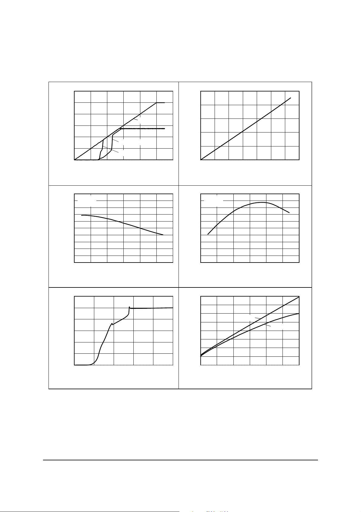
Typical characteristics (ZXCL280 / 5213 shown)
-50 -25 0 25 50 75 100
2.79
2.80
2.81
-50 -25 0 25 50 75 100
23.0
23.2
23.4
23.6
23.8
24.0
24.2
24.4
24.6
24.8
25.0
012345
0
5
10
15
20
25
30
0 25 50 75 100 125 150
20
25
30
35
40
45
50
55
60
0123456
0
1
2
3
4
5
6
0 25 50 75 100 125 150 175
0.00
0.05
0.10
0.15
0.20
0.25
VIN= 3.3V
No Load
Output Voltage v Temperature
Output Voltage (V)
Temperature (˚C)
VIN= 3.3V
No Load
Ground Current v Temperature
Ground Current (µA)
Temperature (˚C)
No Load
Ground Current v Input Voltage
Ground Current (µA)
Input Voltage (V)
VIN= 3.3V
VIN=5V
Ground Current v Load Current
Ground Current (µA)
Load Current (mA)
V
IN
I
OUT
= 100mA
I
OUT
= 1mA
Input to Output Characteristics
Voltage (V)
Input Voltage (V)
Dropout Voltage v Output Current
Dropout Voltage (V)
Output Current (mA)
ZXCL SERIES
Issue 8 - October 2007 5 www.zetex.com
© Zetex Semiconductors plc 2007
Page 6

Typical characteristics
0.0 0.1 0.2 0.3 0.4 0.5
-4
-3
-2
-1
0
1
3
4
5
6
0 102030405060708090100
0
1
2
3
4
5
6
0.0 0.1 0.2 0.3 0.4 0.5
-4
-3
-2
-1
0
1
3
4
5
6
0.0 0.1 0.2 0.3 0.4 0.5
-100
-50
0
50
100
300
350
400
10 100 1k 10k 100k 1M
0.01
0.1
1
10
10 100 1k 10k 100k 1M
0
10
20
30
40
50
60
70
80
0
-20
20
10
-10
C
OUT
= 1μF
Tr & Tf = 2.5μs
Line Rejection IL = 100mA
ΔV
OUT
(mV) V
IN
(V)
Time (ms)
VIN = 5V
IL = 1mA
IL = 100mA
Enable
VIN = 3.3V
IL = 1mA
IL = 100mA
C
OUT
= 1μF
Start-Up Response
Voltage (V)
Time (μs)
C
OUT
= 1μF
Tr & Tf = 2.5μs
0
ΔV
OUT
(mV) V
IN
(V)
-10
10
-20
20
Line Rejection IL = 1mA
Time (ms)
100
50
C
OUT
= 10μF
C
OUT
= 1μF
C
OUT
= 10μF
C
OUT
= 1μF
VIN = 5V
IL = 1mA to 50mA
0
Load Response
ΔV
OUT
(mV) I
L
(mA)
Time (ms)
IL = 100mA, C
OUT
= 1μF
IL = 100mA, C
OUT
= 10μF
No Load, C
OUT
= 10μF
No Load, C
OUT
= 1μF
Output Noise v Frequency
Noise μV/√Hz
Frequency (Hz)
All Caps Ceramic
Surface Mount
IL = 50mA
C
OUT
= 1μF
C
OUT
= 2.2μF
C
OUT
= 10μF
Power Supply Rejection v Frequency
Power Supply Rejection (dB)
Frequency (Hz)
ZXCL SERIES
Issue 8 - October 2007 6 www.zetex.com
© Zetex Semiconductors plc 2007
Page 7

Connection diagrams
V
IN
GND
EN
V
O
NC
Top view
E
N
N/C*
G
ND
V
IN
V
O
Top view
* Should be left open circuit
or connected to pin 3
SC70-5 (H5) SC70-5 (H5)
ZXCLxxx ZXCL5213Vxx
Schematic diagram
ZXCL SERIES
Issue 8 - October 2007 7 www.zetex.com
© Zetex Semiconductors plc 2007
Page 8

ZXCL SERIES
Input to Output Diode
In common with many other LDO regulators, the
ZXCL device has an inherent diode associated
with the output series pass transistor. This diode
has its anode connected to the output and its
cathode to the input. The internal diode is
normally reverse biased, but will conduct if the
output is forced above the input by more than a
VBE (approximately 0.6V). Current will then flow
from V
maximum current in this diode should be
limited to 5mA continuous and 30mA peak. An
external schottky diode may be used to provide
protection when this condition cannot be
satisfied.
to Vin. For safe operation, the
out
Increased Output current
Any ZXCL series device may be used in
conjunction with an external PNP transistor to
boost the output current capability. In the
application circuit shown below, a FMMT717
device is employed as the external pass
element. This SOT23 device can supply up to
2.5A maximum current subject to the thermal
dissipation limits of the package (625mW).
Alternative devices may be used to supply
higher levels of current. Note that with this
arrangement, the dropout voltage will be
increased by the V
Also, care should be taken to protect the pass
transistor in the event of excessive output
current.
drop of the external device.
BE
Scheme to boost output current to 2A
Issue 8 - October 2007 8 www.zetex.com
© Zetex Semiconductors plc 2007
Page 9

Applications information
T
d
T = RCIn
V
V 1.5
d(NOM)
IN
IN
−
⎛
⎝
⎜
⎞
⎠
⎟
Calculation of start up delay as above
Enable control
A TTL compatible input is provided to allow the
regulator to be shut down. A low voltage on the
Enable pin puts the device into shutdown mode.
In this mode the regulator circuit is switched off
and the quiescent current reduces to virtually
zero (typically less than 10nA) for input voltages
above the minimum operating threshold of the
device. A high voltage on the Enable pin ensures
normal operation.
ZXCL SERIES
R
C
The Enable pin can be connected to V
IN
or
driven from an independent source of up to 10V
maximum. (e.g. CMOS logic) for normal
operation. There is no clamp diode from the
Enable pin to V
, so the VIN pin may be at any
IN
voltage within its operating range irrespective
of the voltage on the Enable pin. However input
voltage rise time should be kept below 5ms to
ensure consistent start-up response.
Current Limit
The ZXCL devices include a current limit circuit
which restricts the maximum output current
flow to typically 230mA. Practically the range of
over-current should be considered as minimum
160mA to maximum 800mA. The device’s
robust design means that an output short circuit
to any voltage between ground and V
OUT
can be
tolerated for an indefinite period.
Thermal Overload
Thermal overload protection is included on
chip. When the device junction temperature
exceeds a minimum 125°C the device will shut
down. The sense circuit will re-activate the
output as the device cools. It will then cycle until
the overload is removed. The thermal overload
protection will be activated when high load
currents or high input to output voltage
differentials cause excess dissipation in the
device.
Figure 1 Circuit Connection
Figure 2 Start up delay (T
d
)
Start up delay
A small amount of hysteresis is provided on the
Enable pin to ensure clean switching. This
feature can be used to introduce a start up delay
if required. Addition of a simple RC network on
the Enable pin provides this function. The
following diagram illustrates this circuit
connection. The equation provided enables
calculation of the delay period.
Issue 8 - October 2007 9 www.zetex.com
© Zetex Semiconductors plc 2007
Page 10

Applications information (Cont)
-40-20 0 20406080100
0
100
200
300
400
500
SOT23
SC70
Derating Curve
Max Power Dissipation (mW)
Temperature (°C)
Power dissipation
The maximum allowable power dissipation of
the device for normal operation (P
function of the package junction to ambient
thermal resistance (
temperature (Tj
(T
), according to the expression:
amb
P
max
= (Tj
max
– T
The maximum output current (I
value of Input voltage (V
(V
) is then given by
OUT
θja), maximum junction
), and ambient temperature
max
) /
θ
amb
ja
max
) and output voltage
IN
), is a
max
) at a given
ZXCL SERIES
The dielectric of the ceramic capacitance is an
important consideration for the ZXCL Series
operation over temperature. Zetex recommends
minimum dielectric specification of X7R for the
input and output capacitors. For example a
ceramic capacitor with X7R dielectric will lose 20%
of its capacitance over a -40
range, whereas a capacitor with a Y5V dielectric
loses 80% of its capacitance at -40
85
⬚
C.
An input capacitor of 1
recommended to filter supply noise at the device
input and will improve ripple rejection.
⬚
C to 85⬚C temperature
⬚
C and 75% at
F (ceramic or tantalum) is
I
max
= P
/ (VIN - V
max
OUT
)
The value of qja is strongly dependent upon the
type of PC board used. Using the SC70 package
it will range from approximately 280°C/W for a
multi-layer board to around 450°C/W for a single
sided board. It will range from 180°C/W to
300°C/W for the SOT23-5 package. To avoid
entering the thermal shutdo wn state, Tjmax
should be assumed to be 125°C and Imax less
than the over-current limit,(I
OLIM
). Power
derating for the SC70 and SOT23-5 packages is
shown in the following graph.
Capacitor selection and regulator stability
The device is designed to operate with all types
of output capacitor, including tantalum and low
ESR ceramic. For stability over the full operating
range from no load to maximum load, an output
capacitor with a minimum value of 1
μ
F is
recommended, although this can be increased
without limit to improve load transient
performance. Higher values of output capacitor
will also reduce output noise. Capacitors with
ESR less than 0.5V are recommended for best
results.
The input and output capacitors should be
positioned close to the device, and a ground plane
board layout should be used to minimise the
effects of parasitic track resistance.
Dropout voltage
The output pass transistor is a large PMOS device,
which acts like a resistor when the regulator enters
the dropout region. The dropout voltage is
therefore proportional to output current as shown
in the typical characteristics.
Ground current
The use of a PMOS device ensures a low value of
ground current under all conditions including
dropout, start-up and maximum load.
Power supply rejection and load transient
response
Line and Load transient response graphs are
shown in the typical characteristics.
These show both the DC and dynamic shift in the
output voltage with step changes of input voltage
and load current, and how this is affected by the
output capacitor.
If improved transient response is required, then an
output capacitor with lower ESR value should be
used. Larger capacitors will reduce over/
undershoot, but will increase the settling time.
Best results are obtained using a ground plane
layout to minimise board parasitics.
Issue 8 - October 2007 10 www.zetex.com
© Zetex Semiconductors plc 2007
Page 11

S70-5 Package outline
␣
ZXCL SERIES
Dim. Millimeters Inches Dim. Millimeters Inches
Min. Max. Min. Max. Min. Max. Max. Max.
A 0.80 1.10 0.0315 0.0433 E 2.10 BSC 0.0826 BSC
A1 - 0.10 - 0.0039 E1 1.25 BSC 0.0492 BSC
A2 0.80 1.00 0.0315 0.0039 e 0.65 BSC 0.0255 BSC
b 0.15 0.30 0.006 0.0118 e1 1.30 BSC 0.0511 BSC
C 0.08 0.25 0.0031 0.0098 L 0.26 0.46 0.010 0.018
D 2.00 BSC 0.0787 BSC ␣ 0° 8° 0° 8°
Note: Controlling dimensions are in millimeters. Approximate dimensions are provided in inches
Issue 8 - October 2007 11 www.zetex.com
© Zetex Semiconductors plc 2007
Page 12

ZXCL SERIES
SOT23-5 Package outline
DIM Millimeters Inches
Min. Max. Min. Max.
A 0.90 1.45 0.0354 0.0570
A1 0.00 0.15 0.00 0.0059
A2 0.90 1.30 0.0354 0.0511
b 0.20 0.50 0.0078 0.0196
C 0.09 0.26 0.0035 0.0102
D 2.70 3.10 0.1062 0.1220
E 2.20 3.20 0.0866 0.1181
E1 1.30 1.80 0.0511 0.0708
e 0.95 REF 0.0374 REF
e1 1.90 REF 0.0748 REF
L 0.10 0.60 0.0039 0.0236
a° 0° 30° 0° 30°
Note: Controlling dimensions are in millimeters. Approximate dimensions are provided in inches
Issue 8 - October 2007 12 www.zetex.com
© Zetex Semiconductors plc 2007
Page 13

ZXCL SERIES
Intentionally left blank
Issue 8 - October 2007 13 www.zetex.com
© Zetex Semiconductors plc 2007
Page 14

ZXCL SERIES
Definitions
Product change
Zetex Semiconductors reserves the right to alter, without notice, specifications, design, price or conditions of supply of any product or
service. Customers are solely responsible for obtaining the latest relevant information before placing orders.
Applications disclaimer
The circuits in this design/application note are offered as design ideas. It is the responsibility of the user to ensure that the circuit is fit for
the user’s application and meets with the user’s requirements. No representation or warranty is given and no liability whatsoever is
assumed by Zetex with respect to the accuracy or use of such information, or infringement of patents or other intellectual property rights
arising from such use or otherwise. Zetex does not assume any legal responsibility or will not be held legally liable (whether in contract,
tort (including negligence), breach of statutory duty, restriction or otherwise) for any damages, loss of profit, business, contract,
opportunity or consequential loss in the use of these circuit applications, under any circumstances.
Life support
Zetex products are specifically not authorized for use as critical components in life support devices or systems without the express written
approval of the Chief Executive Officer of Zetex Semiconductors plc. As used herein:
A. Life support devices or systems are devices or systems which:
1. are intended to implant into the body
or
2. support or sustain life and whose failure to perform when properly used in accordance with instructions for use provided in the
labelling can be reasonably expected to result in significant injury to the user.
B. A critical component is any component in a life support device or system whose failure to perform can be reasonably expected to
cause the failure of the life support device or to affect its safety or effectiveness.
Reproduction
The product specifications contained in this publication are issued to provide outline information only which (unless agreed by the
company in writing) may not be used, applied or reproduced for any purpose or form part of any order or contract or be regarded as a
representation relating to the products or services concerned.
Terms and Conditions
All products are sold subjects to Zetex’ terms and conditions of sale, and this disclaimer (save in the event of a conflict between the two
when the terms of the contract shall prevail) according to region, supplied at the time of order acknowledgement.
For the latest information on technology, delivery terms and conditions and prices, please contact your nearest Zetex sales office.
Quality of product
Zetex is an ISO 9001 and TS16949 certified semiconductor manufacturer.
To ensure quality of service and products we strongly advise the purchase of parts directly from Zetex Semiconductors or one of our
regionally authorized distributors. For a complete listing of authorized distributors please visit: www.zetex.com/salesnetwork
Zetex Semiconductors does not warrant or accept any liability whatsoever in respect of any parts purchased through unauthorized sales channels.
ESD (Electrostatic discharge)
Semiconductor devices are susceptible to damage by ESD. Suitable precautions should be taken when handling and transporting devices.
The possible damage to devices depends on the circumstances of the handling and transporting, and the nature of the device. The extent
of damage can vary from immediate functional or parametric malfunction to degradation of function or performance in use over time.
Devices suspected of being affected should be replaced.
Green compliance
Zetex Semiconductors is committed to environmental excellence in all aspects of its operations which includes meeting or exceeding
regulatory requirements with respect to the use of hazardous substances. Numerous successful programs have been implemented to
reduce the use of hazardous substances and/or emissions.
All Zetex components are compliant with the RoHS directive, and through this it is supporting its customers in their compliance with
WEEE and ELV directives.
Product status key:
“Preview” Future device intended for production at some point. Samples may be available
“Active” Product status recommended for new designs
“Last time buy (LTB)” Device will be discontinued and last time buy period and delivery is in effect
“Not recommended for new designs”
“Obsolete” Production has been discontinued
Datasheet status key:
“Draft version” This term denotes a very early datasheet version and contains highly provisional information, which
“Provisional version” This term denotes a pre-release datasheet. It provides a clear indication of anticipated performance.
“Issue” This term denotes an issued datasheet containing finalized specifications. However, changes to
Zetex sales offices
Europe
Zetex GmbH
Kustermann-park
Balanstraße 59
D-81541 München
Germany
Telefon: (49) 89 45 49 49 0
Fax: (49) 89 45 49 49 49
europe.sales@zetex.com
© 2007 Published by Zetex Semiconductors plc
Device is still in production to support existing designs and production
may change in any manner without notice.
However, changes to the test conditions and specifications may occur, at any time and without notice.
specifications may occur, at any time and without notice.
Americas
Zetex Inc
700 Veterans Memorial Highway
Hauppauge, NY 11788
USA
Telephone: (1) 631 360 2222
Fax: (1) 631 360 8222
usa.sales@zetex.com
Asia Pacific
Zetex (Asia Ltd)
3701-04 Metroplaza Tower 1
Hing Fong Road, Kwai Fong
Hong Kong
Telephone: (852) 26100 611
Fax: (852) 24250 494
asia.sales@zetex.com
Corporate Headquarters
Zetex Semiconductors plc
Zetex Technology Park, Chadderton
Oldham, OL9 9LL
United Kingdom
Telephone: (44) 161 622 4444
Fax: (44) 161 622 4446
hq@zetex.com
Issue 8 - October 2007 14 www.zetex.com
© Zetex Semiconductors plc 2007
 Loading...