Diodes ZXBM5210 User Manual
ZXBM5210
REVERSIBLE DC MOTOR DRIVE WITH SPEED CONTROL
Description
The ZXBM5210 is a single chip solution for driving a single-coil
reversible direct current (DC) fans and motors. The integrated full-
bridge driver output stage is designed to minimize audible switching
noise and electromagnetic interference (EMI) providing a low noise
solution
For system flexibility, the device has four modes of operation:
Forward, Reverse, Brake and Standby selected via FWD and REV
pins. The Forward and Reverse modes provide the motor rotation
direction control, the Brake mode allows quick stop and the Standby
mode helps system efficiency by powering down most of the internal
circuits to consume less than 32uA typical. The motor speed can be
adjusted by changing the duty ratio of the PWM signal on the FWD or
REV pins in the PWM mode or alternatively by adjusting DC voltage
NEW PRODUCT
input signal to the V
To help protect the IC and the motor coil the ZXBM5210 includes
under voltage, over voltage, over current and over temperature
protections. Once the safe operating range has been exceeded the
device shuts down the output drive to help prevent over stress on the
IC or the coil. The device internal current protection threshold is 1.5A
typical.
The ZXBM5210 is available in the standard SO8 and thermally
enhanced SO8-EP packages.
pin in the VREF speed control mode.
REF
Features
• Supports single-coil reversible DC motor applications
• Operating voltage: 3V to 18V
• Four modes of operations: Forward, Reverse, Brake and
Standby
• Low quiescent current of 0.85mA typical in normal operation
and 32µA in standby mode
• Internal over current protection
• Under voltage lockout and over voltage protection
• Over temperature protection
• -40°C to +85°C /105°C operating temperature
• 6kV ESD withstand capability
• Standard SO-8 and thermally enhanced SO-8EP
• Totally Lead-Free & Fully RoHS Compliant (Notes 1 & 2)
• Halogen and Antimony Free. “Green” Device (Note 3)
Notes: 1. No purposely added lead. Fully EU Directive 2002/95/EC (RoHS) & 2011/65/EU (RoHS 2) compliant.
2. See http://www.diodes.com/quality/lead_free.html for more information about Diodes Incorporated’s definitions of Halogen- and Antimony-free, "Green"
and Lead-free.
3. Halogen- and Antimony-free "Green” products are defined as those which contain <900ppm bromine, <900ppm chlorine (<1500ppm total Br + Cl) and
<1000ppm antimony compounds.
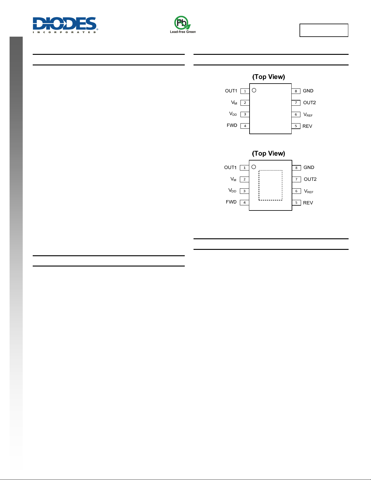
Pin Assignments
SO-8
SO-8EP
Applications
• 5V / 9V/ 12V / 15V DC reversible motors and actuators
• Home appliances
• Handheld power tools
• Valve open and close
• Remote control motorized toys
• Medium Voltage/ Low Power DC Motors
ZXBM5210
Document number: DS36765 Rev. 1 - 2
1 of 17
www.diodes.com
December 2013
© Diodes Incorporated
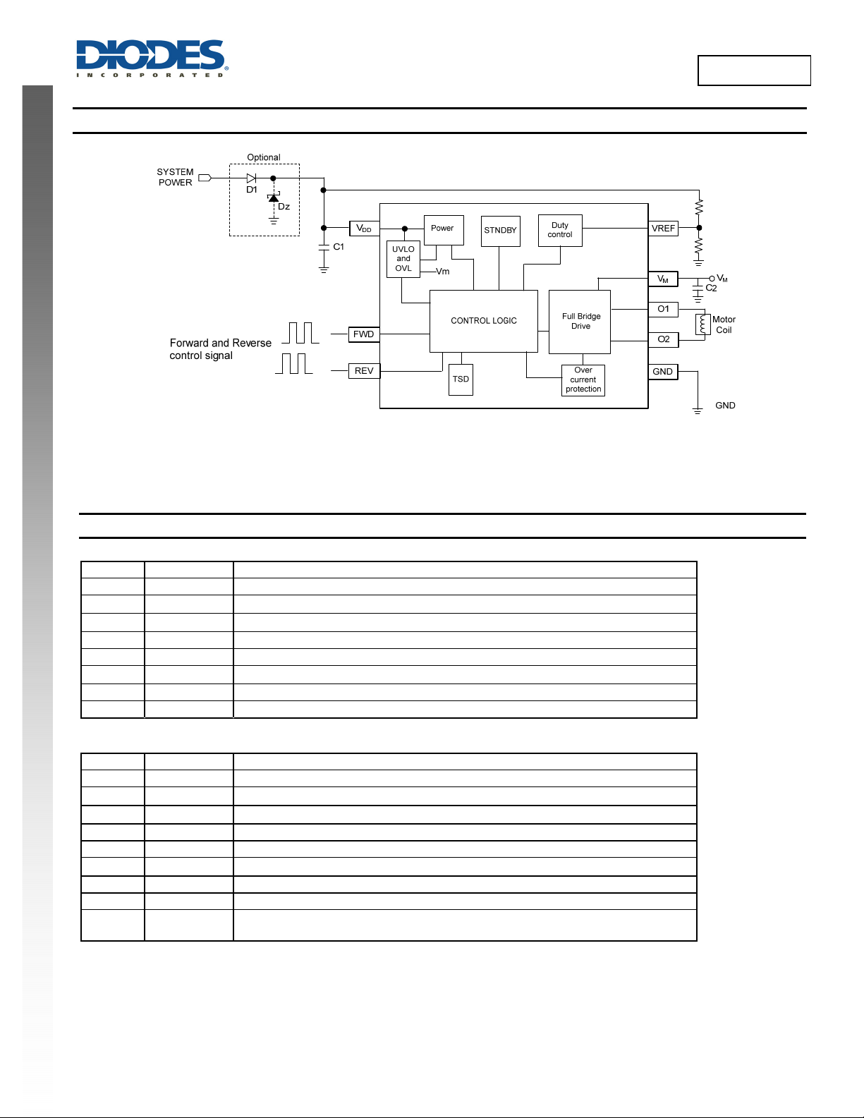
Typical Applications Circuit
ZXBM5210
NEW PRODUCT
Note: 4. C1 is for power stabilization and to strengthen the noise immunity, the recommended capacitance is 100nF to 1µF or more.
C2 is a re-circulating capacitor for back rush voltage and recommended capacitance is 100nF for low current applications to 10µF or more for large
current applications. See application note section
Pin Descriptions
Package: SO-8
Pin # Pin Name Function
1 OUT1 Driver output
2
3
4 FWD Forward Control Input (logic level, 5.5V max)
5 REV Reverse Control Input (logic level, 5.5V max)
6
7 OUT2 Driver Output
8 GND Ground
Package: SO8-EP
Pin # Pin Name Function
1 OUT1 Driver output
2
3
4 FWD Forward Control Input (logic level, 5.5V max)
5 REV Reverse Control Input (logic level, 5.5V max)
6
7 OUT2 Driver Output
8 GND Ground
Pad Pad
V
M
V
DD
V
REF
V
M
V
DD
V
REF
Power Supply Voltage
Power Supply Voltage
Input reference voltage to set the internal PWM oscillator duty ratio
Power Supply Voltage
Power Supply Voltage
Input reference voltage to set the internal PWM oscillator duty ratio
The exposed pad is for thermal dissipation and it is internally connected to the ground.
On the PCB layout, it can be connected to GND or left open circuit.
ZXBM5210
Document number: DS36765 Rev. 1 - 2
2 of 17
www.diodes.com
December 2013
© Diodes Incorporated
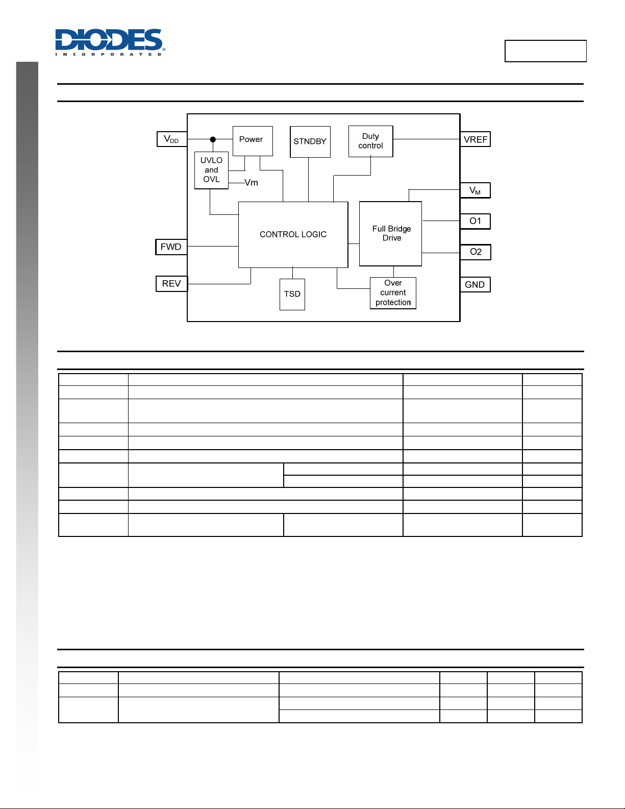
Functional Block Diagram
NEW PRODUCT
ZXBM5210
Absolute Maximum Ratings (Note 5) @T
Symbol Characteristic Values Unit
VM and V
V
OUT1, VOUT2
V
REF
V
and V
FWD
V
REVERSE
I
OUTPUT
PD
Ts Storage temperature range -65 to +150
TJ
ESD HBM
Notes: 5. Stresses greater than the 'Absolute Maximum Ratings' specified above, may cause permanent damage to the device. These are stress ratings
only; functional operation of the device at these or any other conditions exceeding those indicated in this specification is not implied. Device
reliability may be affected by exposure to absolute maximum rating conditions for extended periods of time
6. The absolute maximum supply voltage of 24V is a transient stress rating and is not meant as a functional operating condition. It is not recommended
7. SO-8 soldered to minimum recommended landing pads (see Package Outline Dimension section) on a 1”x1” two-layer 2oz.copper FR4 PCB
8. SO-8EP exposed pad soldered to minimum recommended landing pads (see Package Outline Dimension section) on a 2”x2” two-layer 2oz.copper
Supply voltage (Note 6) 24 V
DD,
All other pins except FWD and REV pins 24 V
FWD and REV pin voltage 7 V
REV
Reverse supply Voltage on all pins -0.3 V
Output current (source and sink)- Peak 1500 mA
Package power dissipation
Maximum junction temperature 150
Human Body Model ESD withstand
capability
to operate the device at the absolute maximum rated conditions for any period of time.
(1.6mm thickness) without any via or copper flood on the bottom layer. See thermal de-rating curves in the thermal performance section.
FR4 PCB (1.6mm thickness) with four thermal vias in the exposed PAD to the copper flood on the bottom layer. See thermal de-rating curves in the
thermal performance section.
= +25°C, unless otherwise specified.)
A
SO8 (Note 7) 1043 mW
SO8-EP (Note 8) 2980 mW
, VM, V
V
DD
GND and OUT1 OUT2 pins
, FWD, REV,
REF
6 kV
°C
°C
Recommended Operating Conditions
Symbol Characteristic Conditions Min Max Unit
VDD
TA
Supply Voltage Operating 3
Operating Temperature Range
ZXBM5210
Document number: DS36765 Rev. 1 - 2
Operating, SO8 package -40
Operating, SO8-EP package -40
3 of 17
www.diodes.com
18
+85
+105
December 2013
© Diodes Incorporated
V
°C
°C
ZXBM5210
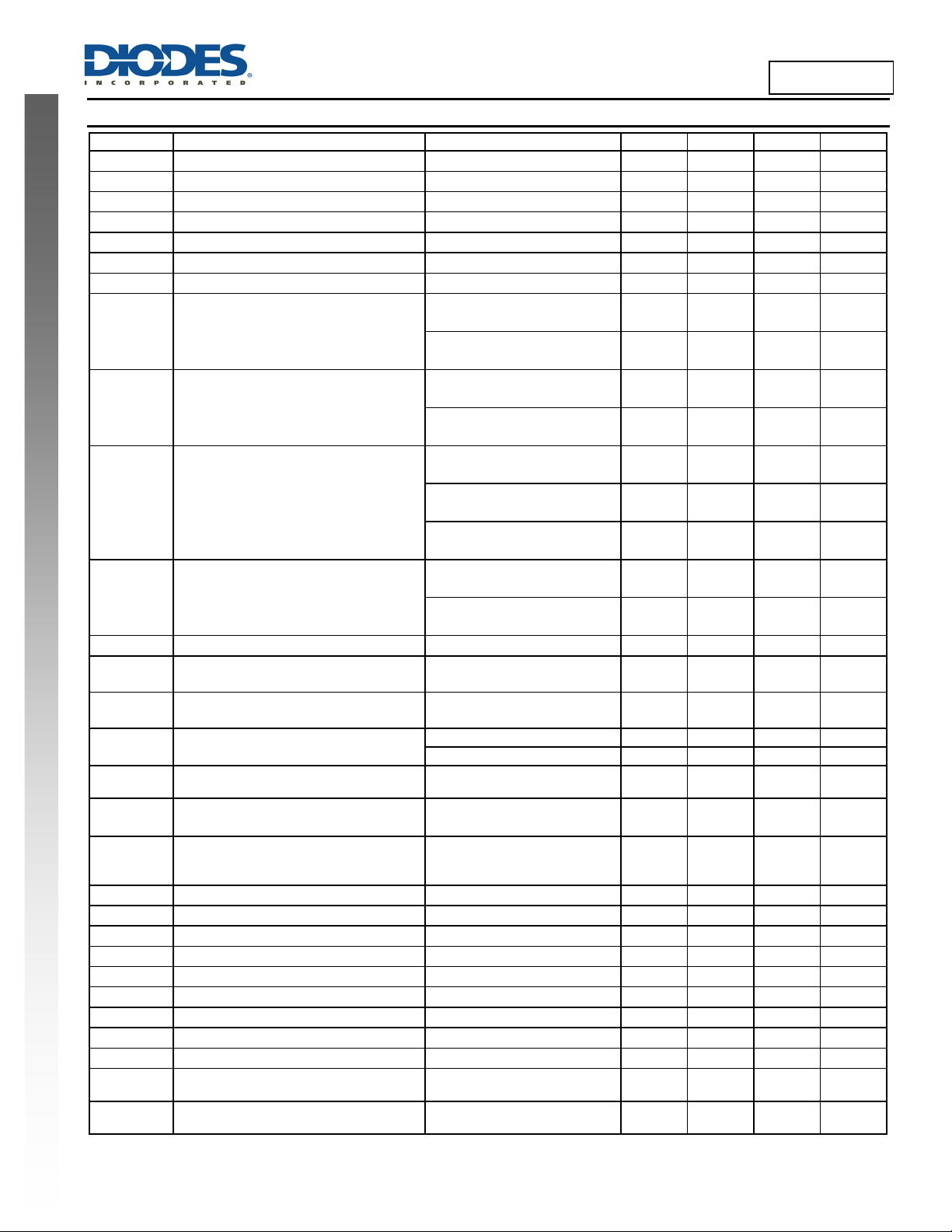
Electrical Characteristics (Note 9)(@T
= +25°C, VDD = 12V, unless otherwise specified.)
A
Symbol Characteristics Conditions Min Typ Max Unit
IDD
I
DD_STNDBY
V
UV_TH
V
UVLO_R
V
UV_HYS
V
OV_TH
V
OV_RLTH
VOH
VOL
NEW PRODUCT
VOH+ VOL
R
ON_Total
I
LIM_TH
V
REF
I
VREF
F
OUT
F
FWD_REV
T
DEAD
t
SDN_DELAY
V
FWDH
V
FWDL
I
FWDH
I
FWDL
V
REVH
V
REVL
I
REVH
I
REVL
D
PWM_MIN
Tj_
SDN_TH
Tj_
SDN_HYST
Note: 9. Typical data is at TA = +25°C, VDD = 12V. The maximum and minimum parameters values over the operating temperature range are not tested in
production, they are guaranteed by design, characterization and process control.
ZXBM5210
Document number: DS36765 Rev. 1 - 2
Supply Current No Load — 0.85 2.5 mA
Standby Supply Current FWD=REV=LOW (GND)
Under Voltage lock Out Threshold Voltage Decreasing
Under Voltage Lock Out Release Threshold Voltage Increasing
Under Voltage Hysteresis Voltage Increasing
Overvoltage Threshold Voltage Increasing
Overvoltage Release Threshold Voltage Decreasing 17.0 19 — V
= 300mA,
I
OUT
= -40°C to +105°C
T
Output Voltage High
Output Voltage Low
Output voltage of N- and PMOS and bond
wire voltage drop combined
Combined N- and PMOS R
bond wire resistance
Over current protection threshold 1.2 1.5 A
V
voltage range
REF
( DC voltage speed control mode)
V
bias current
REF
( DC voltage speed control mode)
Output PWM switching frequency
(Internal PWM oscillator)
Input PWM frequency of speed control
signal
Dead time between current reversal
DSON
including
Shutdown delay – Internal circuits active
after FWD = REV = L
(except from brake mode)
FWD Input H Level 2 — 5.5 V
FWD Input L Level 0 — 0.8 V
FWD pin current – H Level
FWD pin current – L Level
REV Input H Level 2 — 5.5 V
REV Input L Level 0 — 0.8 V
REV pin current – H Level
REV pin current – L Level
Output minimum duty ratio 0% 100 %
IC junction temperature thermal shutdown
threshold
IC junction temperature thermal shutdown
hysteresis
A
I
=500mA
OUT
= -40°C to +105°C
T
A
= 300mA,
I
OUT
= -40°C to +105°C
T
A
I
= 500mA,
OUT
T
= -40°C to +105°C
A
I
= 300mA,
OUT
= -40°C to +105°C
T
A
I
= 500mA,
OUT
= -40°C to +105°C
T
A
I
= 300mA, VDD = 3V
OUT
= -40°C to +105°C
T
A
I
= 500mA,
OUT
= -40°C to +105°C
T
A
I
= 300mA, VDD = 3V
OUT
= -40°C to +105°C
T
A
3 —
= VDD
V
REF
VREF control mode 20 26.5 35 kHz
PWM speed control mode 20 — 100 kHz
PWM control mode 20 — 100 kHz
V
= 3V to 18V
DD
= -40°C to +105°C
T
A
FWD = GND
REV = GND
FWD pin: V
FWD pin: V
REV pin: V
REV pin: V
FWD
FWD
RVS
RVS
= 5V
= 0V
= 5V
= 0V
— 165 —
— 25 —
—
—
—
—
—
V
- 0.25 VDD - 0.15
DD
V
- 0.43 VDD - 0.25
DD
32 45 uA
2.6 — V
2.8 3.0 V
200 — mV
20.7 24 V
— 0.15 0.25 V
— 0.25 0.43 V
— 0.3 0.5 V
— 0.5 0.86 V
— 0.39 0.66 V
— 1 1.72
— 1.3 2.2
(18V max)
-15 0 15 μA
2.1 3 3.9 μs
125 180 — μs
— 50 — μA
— 50 — μA
— 50 — μA
— 50 — μA
4 of 17
www.diodes.com
— V
— V
Ω
Ω
V
DD
© Diodes Incorporated
V
o
C
o
C
December 2013
ZXBM5210
Application Note
Rotation Control and Standby Modes
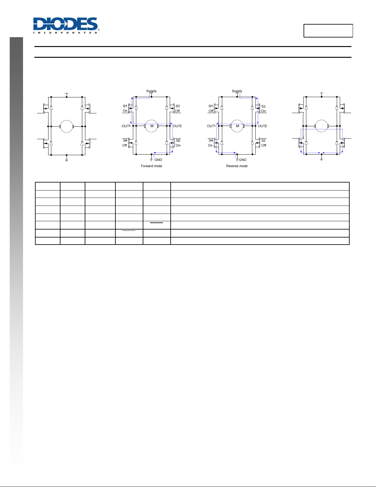
The device has FWD and REV pins for controlling the motor rotation directions. The device has four motor operation modes: 1) Standby mode,
2) Forward mode, 3) Reverse mode and 4) Brake mode. The four modes are controlled by the FWD and REV logic pins.
Supply
Supply
S1
OUT1
S4
On
Brake mode
NEW PRODUCT
S1
Off
OUT1 OUT2
Off
M
GND
Standby mode
S3
Off
S2S4
Off
FWD REV
V
REF
OUT1 OUT2 Operating mode
L L x Open Open Standby mode – All switches are off
H L
L H
3V to V
3V to V
DD
DD
H L
L H
Forward mode – Current flows from OUT1 to OUT2; V
Reverse mode – Current flows from OUT2 to OUT1; V
duty control
REF
duty control
REF
H H x L L Brake mode – Short circuit brake with low side switches on
PWM L
L PWM
V
DD
V
DD
H PWM
PWM H
Forward mode – Current flows from OUT1 to OUT2; PWM control mode
Reverse mode – Current flows from OUT2 to OUT1; PWM control mode
H H x L L Brake mode – Short circuit brake with low side switches on
In the brake mode, switches S2 and S4 are ON allowing the motor to stop quickly. All the internal control circuits are fully operational.
In the standby mode all the output drive switches are off and additionally, the internal circuits are also turned off to minimize power consumption.
The power consumption in the standby mode is less than in the brake mode. If running motor enters the Standby mode, due to the body diodes
the motor free wheels to idle state. Whenever the motor enters the standby mode from any mode (except the brake mode) the control logic will
remain active in previous mode for at least 125µs before shutting down the internal circuits. To prevent device entering the standby mode during
operating mode changes, the mode change signals should be completed within 125µs.
In the forward mode, with switches S1-S2 ON and S3-S4 OFF, OUT1 is high and OUT2 is low. The motor current flows from OUT1 to OUT2. In
the reverse mode, switches S1-S4 are ON while S1-S2 are OFF to allow motor current flow from OUT2 to OUT1.
In the forward or reverse mode, for V
speed control, the output drive duty ratio is generated internally based on the voltage on the V
REF
For PWM speed control, external PWM signals applied to the FWD or REV pins control the PWM switching of the low side S2 (forward mode)
or S4 (reverse mode). See application section for further details.
The ZXBM5210 has three modes of speed control: V
speed control mode, PWM speed control mode and by adjusting the supply voltage
REF
S3
OffOf f
M
GND
OUT2
S2
On
pin.
REF
ZXBM5210
Document number: DS36765 Rev. 1 - 2
5 of 17
www.diodes.com
December 2013
© Diodes Incorporated
ZXBM5210
Application Note (cont.)
Motor Speed Control with DC Voltage on V
Motor speed can be controlled by adjusting the DC voltage into the V
voltage to the supply V
voltage.
DD
In V
speed control mode, FWD and REV pins are only used for direction control and therefore high frequency PWM control signal should not
REF
be applied to the FWD and REV pins. If repetitive direction changes required, it is recommended to keep direction change frequency of below
400Hz.
The speed and direction control is given by:
FWD REV
V
REF
OUT1 OUT2
L L x Open Open Standby mode – All switches are off
NEW PRODUCT
H L
H L
L H
L H
V
DD
3V to V
V
DD
3V to V
DD
DD
H H x L L Brake mode – Short circuit brake with low side switches on
H L
H L
L H
L H
Motor Speed Control with a PWM Input Signal
Motor speed can be controlled by adjusting the duty cycle of the PWM speed control signal into the FWD or REV while keeping the VDD pin at
the nominal motor voltage. In this mode the input voltage on the V
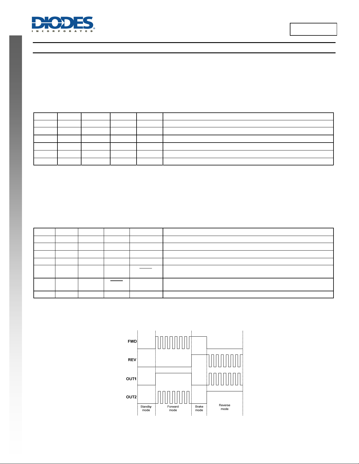
In PWM speed control mode the high side switches S1 and S3 are kept fixed while the low side switches S2 or S4 are switched. In the forward
mode, S1 is kept switched on, S2 is switched in accordance with the PWM signal and S3 and S4 are switched off. In reverse mode, S3 is
switched on, S4 is switched in accordance with the PWM signal and S1 and S2 are switched off.
The speed and direction control is given by:
FWD REV
V
REF
L L x Open Open Standby mode – All switches are off
H L
L H
V
DD
V
DD
H H x L L Brake mode – Short circuit brake with low side switches on
PWM L
L PWM
V
DD
V
DD
H H x L L Brake mode – Short circuit brake with low side switches on
The motor speed is proportional to the input PWM signal duty. For example, for a 12V motor the V
PWM control signal duty to adjust the motor speed linearly. The timing diagram below shows the output O1 and O2 in relation to PWM speed
control signal at PWM pin.
OUT1 OUT2 Operating mode
H L
L H
H PWM
PWM H
REF
Pin
pin. The output drive PWM duty ratio is defined by the ratio of the V
REF
Operating mode
Forward mode – Current flows from OUT1 to OUT2; 100% duty
Forward mode – Current flows from OUT1 to OUT2; V
duty control
REF
Reverse mode – Current flows from OUT2 to OUT1; 100% duty
Reverse mode – Current flows from OUT2 to OUT1; V
pin must be greater than or equal to VDD.
REF
duty control
REF
Forward mode – Current flows from OUT1 to OUT2; 100% duty
Reverse mode – Current flows from OUT2 to OUT1; 100% duty
Forward mode – Current flows from OUT1 to OUT2;
PWM control mode
Reverse mode – Current flows from OUT2 to OUT1
PWM control mode
pin is maintained at 12V while varying the
DD
REF
Frequency of PWM speed control signal can be between 8kHz to 100kHz. Recommended typical PWM signal frequency is 25kHz to keep
switching frequency away from the audible band.
ZXBM5210
Document number: DS36765 Rev. 1 - 2
6 of 17
www.diodes.com
December 2013
© Diodes Incorporated
 Loading...