

Page 1
Description
The ZXBM2004 is a 2-phase, Brushless Direct Current (BLDC)
motor control pre-driver with variable PWM speed control
suitable for fan and blower motors.
For system flexibility, motor speed can be controlled by
changing SPD pin voltage which can be either from Thermistor
network, external voltage or PWM signal.
To help protect the motor coil, the ZXBM2004 provides Rotor
Lock Protection which shuts down the output drive if rotor lock
is detected. The device automatically re-starts when the rotor
lock is removed.
NEW PRODUCT
A Tachometer output is provided by open-drain Frequency
Generator (FG) Pin which allows external interface to monitor
motor rotation or speed. The FG output is the magnetic
change frequency.
The ZXBM2004 is available in small space saving low prof ile
U-QFN3030-16 and QSOP-16 packages.
Features
• Supports two-phase BLDC motor control
• Operating voltage: 4.7V to 18V
o Can be extended with external regulator
• PWM speed control via external Thermister, DC voltage or
PWM signals
• Reference voltage output
• Built-in Hall amplifier allows direct connection of Hall
element
• Rotor Lock Protection (Lock detection, output shutdown
and automatic re-start)
• Rotor lock detect (RD) output
• Minimum speed setting
• Frequency generator (FG) output for speed measurements
• Low noise
• Space saving low profile U-QFN3030-16 and QSOP-16
packages
• “Green” Molding Compound
ZXBM2004
TWO PHASE VARIABLE SPEED
MOTOR CONTROL PRE-DRIVER
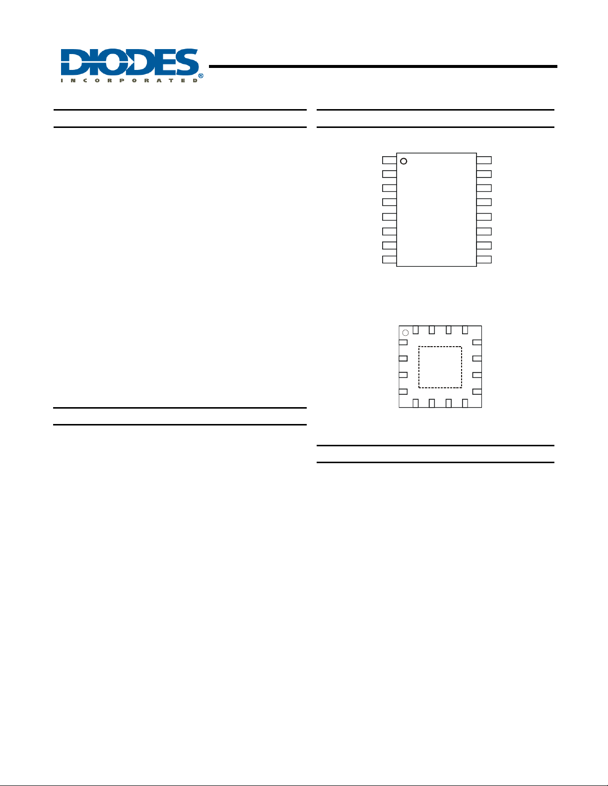
Pin Assignments
(Top View)
Ph1
Ph2
NC
FG
V
CC
V+OP
Ph1
Ph2
N/C
FG
RD
C
LCK
1
H+
H-
N/C
ThRef
SPD
C
PWM
S
MIN
GND
ZXBM2004
QSOP-16
(Top View )
CC
V+OP
V
H+
H-
NC
ThRef
SPD
C
PWM
MIN
S
GND
U-QFN3030-16
C
LCK
RD
Applications
• Desktop PC and Servers fans and blowers
• Instrumentation fans
• Central heating blowers
• Automotive instrument cooling and climate control
• Extractor fans
• General motors and pumps
ZXBM2004
Document number: DS33433 Rev. 5 - 2
1 of 19
www.diodes.com
February 2012
© Diodes Incorporated
Page 2
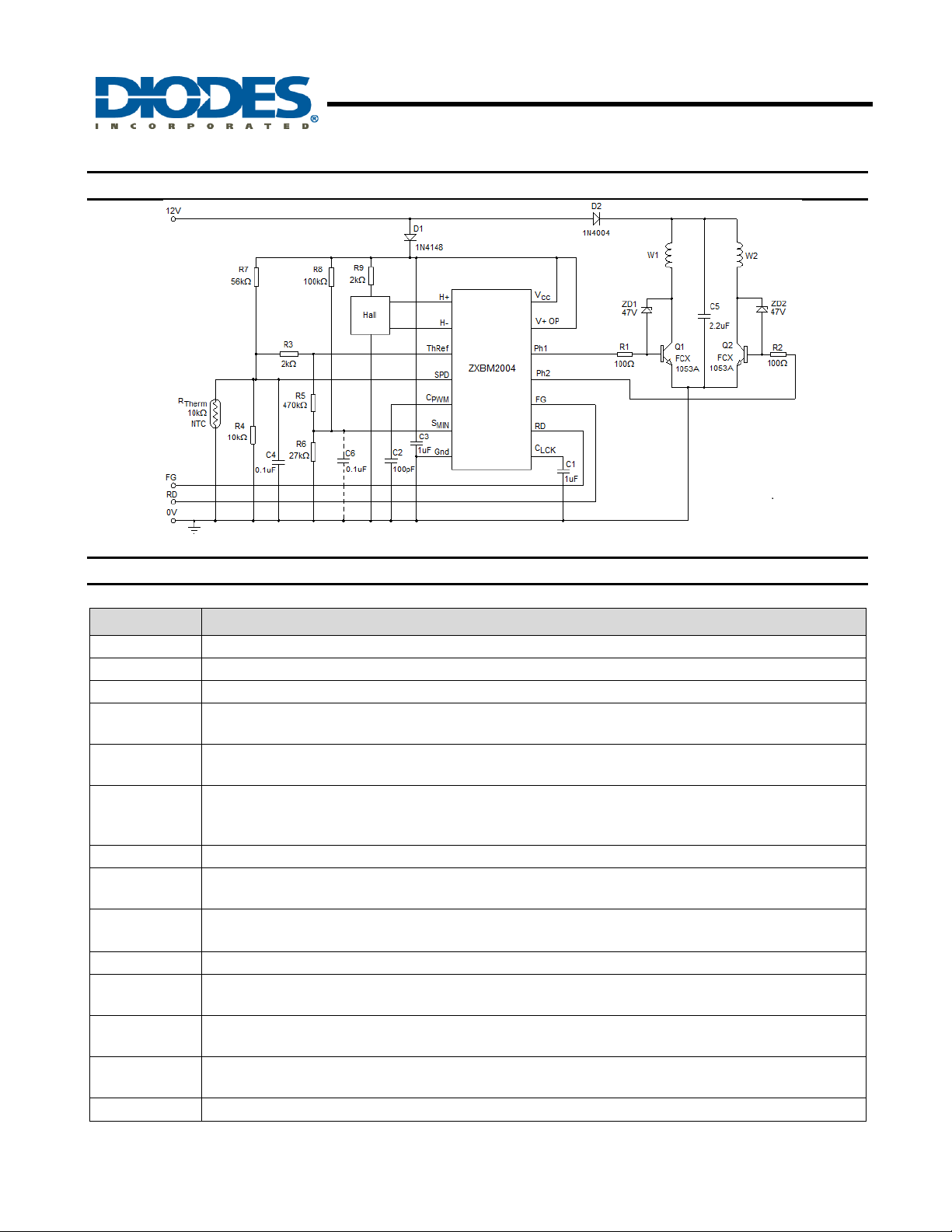
Typical Application Circuit
NEW PRODUCT
ZXBM2004
TWO PHASE VARIABLE SPEED
MOTOR CONTROL PRE-DRIVER
Pin Descriptions
Pin Name Description
H+ Hall input to non-inverting input of internal operational amplifier
H- Hall input to inverting input of internal operational amplifier
ThRef Reference output voltage
SPD
C
PWM
S
MIN
GND Supply return ground pin
C
LCK
RD
FG Frequency Generator output to provide a tachometer signal
Ph1
Ph2
V+OP
VCC
ZXBM2004
Document number: DS33433 Rev. 5 - 2
Speed control pin; The control signal voltage should be bet ween 3V to 1V for 0% to 100 % (full speed)
speed control
PWM frequency setting pin: Connect a capacitor from this pin to ground (0V) to set PWM frequency.
Capacitor of 0.1nF will give PWM frequency of 24kHz typical.
Minimum speed setting pin: Voltage between 3V to 1V on this pin sets the minimum speed
between 0% to full speed. Lowest minimum speed achieved depends on the motor coil
design.
Rotor lock detect and auto re-start timing pin: Connect a capacitor from this pin to ground to set the lock
detect and restart timing.
Rotor lock detect pin: Open collector output to indicate rotor lock detection
Connect a pull-up resistor from the pin to the pull-up supply rail
Phase-1 low-side external power switch drive output pin: Darlington emitter follower output with active
pull down to give source/sink current of 80mA/16mA
Phase-2 low-side external power switch drive output pin: Darlington emitter follower output with active
pull down to give source/sink current of 80mA/16mA
Phase output supply voltage pin: The pin allows to optimiz e the supply to output drive depending on
whether external power switch is Bipolar switch or MOSFET
Power supply pin
2 of 19
www.diodes.com
February 2012
© Diodes Incorporated
Page 3
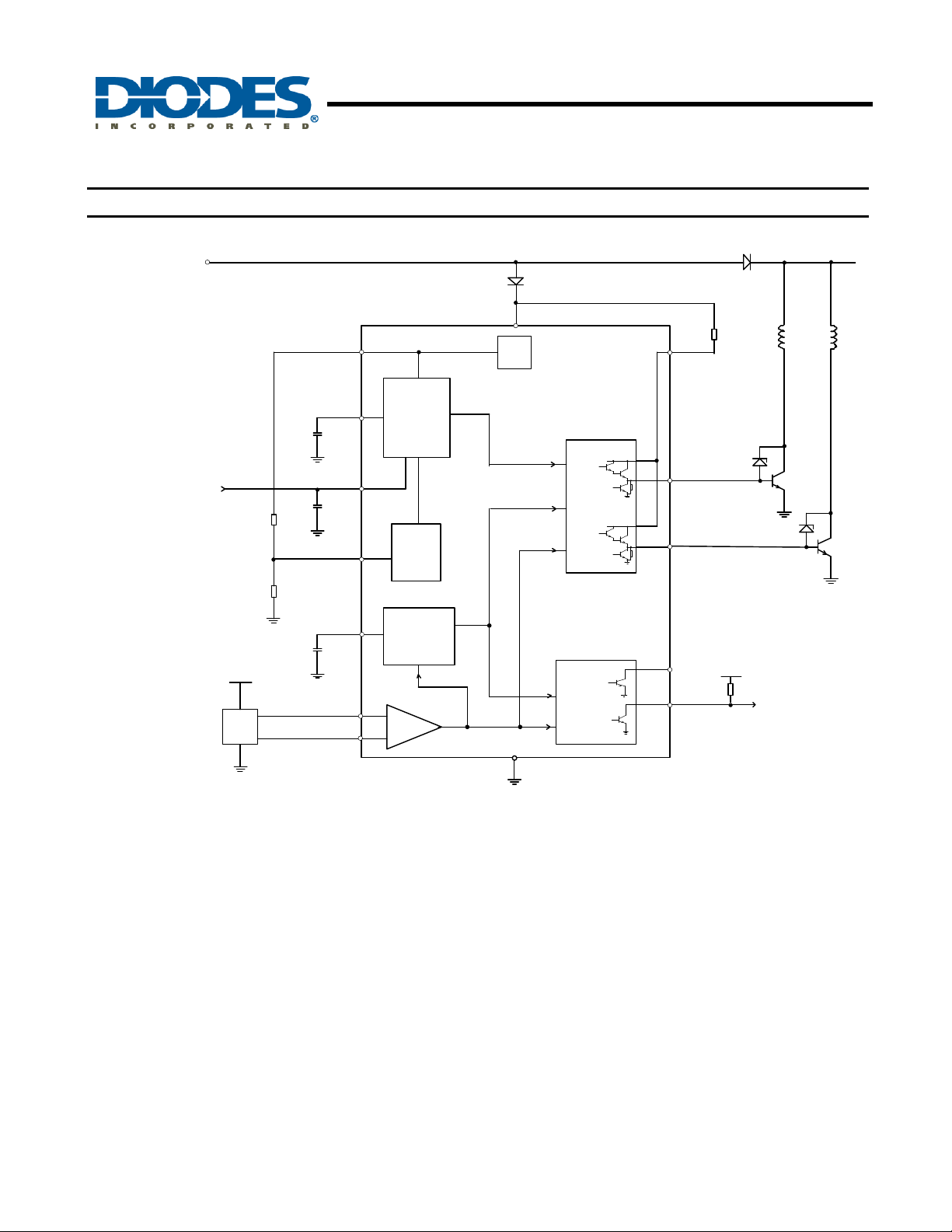
Functional Block Diagram (Note 1)
Supply Voltage
NEW PRODUCT
V
Speed Control Voltage
SPD
ThRef
C
PWM
SPD
SMIN
PWM Osc
Set Min
Speed
D1
Vref
ZXBM2004
TWO PHASE VARIABLE SPEED
MOTOR CONTROL PRE-DRIVER
D2
V
CC
Phase
Drive &
Control
V+OP
Set Phase Drive
Current Limit
Vcc
Ph1 Lo
Vcc
Ph2 Lo
L1
L2
Locked
Rotor
Detect
Hall
Amp
GND
Speed &
Lock
Detect
RD
FG
Vcc
Hall Bias
Hall
C
LCK
H+
H-
Notes: 1. The ZXBM2004 has an open-collector FG and RD. Typically a pull-up resistor of 10kΩ is recommended from FG or RD pin to the supply voltage.
ZXBM2004
Document number: DS33433 Rev. 5 - 2
3 of 19
www.diodes.com
February 2012
© Diodes Incorporated
Page 4
ZXBM2004
Absolute Maximum Ratings (T
Symbol Characteristics Values Unit
V
Note: 2. Stresses greater than the 'Absolute Maximum Ratings' specified above, may cause permanent damage to the device. These are stress ratings only;
functional operation of the device at these or any other conditions exceeding those indicated in this specification is not implied. Device reliability
may be affected by exposure to absolute maximum rating conditions for extended periods of time.
NEW PRODUCT
3. U-QFN3030-16 dissipation is based on a two-layer 2oz. copper 2”x 2” FR4 substrate PCB with thermal vias to the bottom layer.
CCMAX
I
CCMAX
P
DMAX
TA
T
STG
Supply voltage -0.6 to +20 V
IC input current 100 mA
Power Dissipation (Note 4)
Operating ambient temperature -40 to +110
Storage Temperature Range -55 to +150
Recommended Operating Conditions (T
Symbol Parameter Conditions Min Max Unit
VCC
TA
Supply Voltage Operating
Operating Temperature Range Operating
Electrical Characteristics (T
Symbol Characteristics Conditions Min Typ. Max Unit
ICC
Supply Current No Load (Note 4) - 5.5 7.5 mA
VIN Hall amplifier input voltage Diff peak to peak 40 mV
VCM
V
VOH
V
V
IOH
I
PWMC
I
PWMD
V
V
F
Notes: 4. Measure with pins H+, H-, C
5. Measured when opposing Phase Output is Low
Hall amplifier common mode voltage 0.5
Hall amplifier input offset voltage ±7 mV
OFS
IBS
Hall amplifier bias current 400 700 nA
Ph1 and Ph2 output high voltage
Ph1 and Ph2 output low voltage
OLA
Ph1 and Ph2 output low voltage
OLB
Ph1 and Ph2 output source current 80 mA
IOL
Ph1 and Ph2 output sink current 16 mA
C
C
C
THH
C
THL
PWM
6. Measured when opposing Phase Output is High
charge current
PWM
discharge current
PWM
high threshold voltage
PWM
low threshold voltage
PWM
PWM frequency
LCK
and C
= 25°C, unless otherwise noted, Note 2)
A
QSOP-16 500
U-QFN3030-16 (Note 3) 1500
= 25°C)
A
= 25°C, V
A
CC
= 12V)
I
= 80mA V
OH
=16mA (Note 5)
I
OH
I
= 50uA (Note 6)
OH
4.5 7.85 µA
38 65 µA
3 V
1 V
C
= 0.1nF
PWM
and all other signal pins open circuit
PWM
TWO PHASE VARIABLE SPEED
MOTOR CONTROL PRE-DRIVER
4.7
-40
-2.2
CC
Vcc -1.8 V
0.4 0.6 V
0.4 0.6 V
24 kHz
18.0 V
+110
V
-1.5
CC
mW
oC
o
C
o
C
V
ZXBM2004
Document number: DS33433 Rev. 5 - 2
4 of 19
www.diodes.com
February 2012
© Diodes Incorporated
Page 5
Electrical Characteristics (cont.) (T
Symbol Characteristics Conditions Min Typ. Max Unit
V
ThRef reference output voltgae
ThRef
I
ThRef output current 1 mA
SPDL
SPDH
ISPD
S
C
C
input current V
MIN
SPD voltage minimum 100% PWM drive 1 V
SPD voltage maximum 0% PWM drive 3 V
SPD voltage maximum
charge current
LCK
discharge current
LCK
high threshold voltage
low threshold voltage
Lock condition On:Off ratio 1:12
FG Low level output current 5 mA
FG Low level output voltage
FGOL
RD Low level output current 5 mA
RD Low level output current
RDOL
tCD
Commutation delay 7.5 µs
NEW PRODUCT
OThRef
I
ISMIN
V
V
I
I
LCKC
I
LCKD
V
CLCKTHH CLCK
V
CLCKTHL CLCK
I
FGOL
V
I
RDOL
V
= 25°C, V
A
ZXBM2004
TWO PHASE VARIABLE SPEED
MOTOR CONTROL PRE-DRIVER
= 12V)
CC
I
= 100µA
OThRef
= 2V, SPD=open
IN
V
= 2V
IN
2.8 3.8 µA
4.6 054 µA
3 V
1 V
I
= 5mA
FGOL
I
= 5mA
RDOL
2.88 2.96 3.10 V
-0.25 -0.3 µA
0.8 2 µA
0.5 V
0.5 V
ZXBM2004
Document number: DS33433 Rev. 5 - 2
5 of 19
www.diodes.com
February 2012
© Diodes Incorporated
Page 6

ZXBM2004
Functional Descriptions
H+ and H- Hall Inputs
The rotor position is detected by a Hall sensor, with the output applied to the H+ and H-pins. This sensor can be either a 4 pin
'naked' Hall device or of the 3 pin buffered switching t ype. For a 4 pin dev ice the di fferential Ha ll output signal is co nnec ted to
the H+ and H-pins. For a buffered Hall sensor the Hall device output is attached to the H+ pin, with a pull-up attached if
needed, whilst the H-pin has an external potential divider attached to hold the pin at half V
H-, Ph2 is the active drive.
ThRef - Output Reference Voltage
This is a reference voltage of nominal 3V. It is designed for the abil ity to 'source' and therefore it will not 'sink' any current
from a higher voltage. The current drawn from the pin by the minim um speed potential divider to pin S
setting network should not exceed 1mA in total at maximum temperature.
NEW PRODUCT
SPD - Speed Control Input
The voltage applied to the SPD pin provides control over motor spee d by varying the Pulse Width Modulated (PWM) drive
ratio at the Ph1 and Ph2 outputs. The control signal takes the form of a voltage input of range 3V to 1V, representing 0% to
100% drive respectively.
If variable speed control is not required this pin can be left with an external potential divider to set a fixed sp eed or tied to
ground to provide full speed i.e. 100% PWM drive.
If required this pin can also be used as an enable pin. The application of a voltage >3.0V will force the PWM drive fully off, in
effect disabling the drive.
S
– Minimum Speed Setting
MIN
A voltage can be set on S
pin such that internally SPD voltage cannot rise above S
speed it therefore restricts the lower speed range of the fan. If this feature is not required the pin is left tied to ThRef so no
minimum speed will be set.
If the fan is being controlled from an external voltage source onto the SPD pin then either this feature should not be used or if
it is required then a resistor greater than 1kΩ should be placed in series with the SPD pin.
C
– Output PWM Frequency Setting
PWM
This pin has an external capacitor attached to set the PWM frequency for the Phase drive outputs. A cap acitor value of 0.1nF
will provide a PWM frequency of typically 24kHz. The C
()()
PWM
T
=
Where: C = (C
V
THH
I
PWMC
T
As these threshold voltages are nominally set to V
PWM
T +=
PWM
I
and V
C2
THLTHH
PWMC
I
PWM
and I
is in ms
PWMDPWMC
I
+15) in pF
THL
PWMD
C2
pin via a potential divider between the ThRef and Gnd. This voltage is monitored by the SPD
MIN
voltage. As a higher voltage on the SPD pin represents a lower
MIN
timing period (T
PWM
THLTHH
CVV
×−
+
are the C
are the charge and discharge currents in µA.
PWMD
I
PWM
CVV
×−
pin threshold voltages
= 3V and V
THH
= 1V the equations can be simplified as follows:
THL
TWO PHASE VARIABLE SPEED
MOTOR CONTROL PRE-DRIVER
. When H+ is high in relation to
CC
and any voltage
MIN
) is determined by the following equation:
PWM
ZXBM2004
Document number: DS33433 Rev. 5 - 2
6 of 19
www.diodes.com
February 2012
© Diodes Incorporated
Page 7

ZXBM2004
Functional Description (cont.)
- Locked Rotor Timing Capacitor
C
LCK
Should the fan stop rotating for any reason, i.e. an obstruction i n the fan blade or a seized bearing, the n the device will ent er
a Rotor Locked condition. In this condition after a predetermined time (T
will be disabled. After a further delay (T
attempt to re-start the fan. This cycle of (T
GND – Supply Return
This is the device supply ground return pin and will generally be the most negative suppl y pin to the fan.
RD - Rotor Lock Detect Output
NEW PRODUCT
This pin is the Locked Rotor status output as referred to in the C
and low when it is running.
This is an open collector drive giving an active pull down with the high level being provide d b y an external pull up resistor.
) the controller will re-enable the Phase drive for a defined period (TON) in an
OFF
) and (TON) will be repeated indefinitely or until the fan re-starts.
OFF
timing section above. It is high when the rotor is stopped
LCK
TWO PHASE VARIABLE SPEED
MOTOR CONTROL PRE-DRIVER
) the RD pin will go high and the Phase outputs
LOCK
Hall
V
THH
C
LCK
V
THL
T
T
Lock
T
Off
On
RD
FG
FR and RD Timing Diagram
ZXBM2004
Document number: DS33433 Rev. 5 - 2
7 of 19
www.diodes.com
February 2012
© Diodes Incorporated
Page 8

ZXBM2004
Functional Descriptions (cont.)
FG -Frequency Generator (tachometer) Output
This is the Frequency Generator output and is a buffered signal from the Hall sensor.
This is an open collector drive giving an active pull down with the high level being provi ded by an external pull up resistor.
Ph1 and Ph2 Output Drives
This pair of outputs drives the external devices. These outputs provide both the commutation and PWM waveforms. The
outputs are of the Darlington emitter follower type with an active pull-down to help faster switch off when using bipolar
devices. When in the high state the outputs will provide up to 80mA of drive into the base or gates of external tra nsistors as
shown in the Typical Application circuit following.
When in the low state the active Phase drive is capable of sinking u p to 16mA when driving low to aid turn off times during
NEW PRODUCT
PWM operation. When the Phase is inactive the output is held low by an internal pull-down resistor.
V+OP Phase Outputs Supply Voltage
This pin is the supply to the Phase outputs and will be connected differently dependant upon external transistor type . For
bipolar devices this pin will be connected by a resistor to the V
transistor base so its value is chosen accordingly. For MOSFET devices the pin will connect directly to the V
V
– Supply Voltage
CC
This is the device internal circuitry supply voltage. For 5V to 12V fans this can be supplied directly from the Fan Motor suppl y.
For fans likely to run in excess of the 18V maximum rating f or the device t his will be s upplied from an external regulat or such
as a Zener diode.
pin. The resistor is used to control the current into the
CC
TWO PHASE VARIABLE SPEED
MOTOR CONTROL PRE-DRIVER
CC
pin.
ZXBM2004
Document number: DS33433 Rev. 5 - 2
8 of 19
www.diodes.com
February 2012
© Diodes Incorporated
Page 9

ZXBM2004
Application Note
The ZXBM2004 is primarily controlled by a voltage o n the SPD pin. A voltage of 1V represents a 100% PWM at the P hase
Outputs and in turn represents full speed. 3V on the SPD pin conversely repres ents 0% PWM. The motor can therefore be
controlled simply by applying a control voltage onto the SPD pin with the minimal use of external components.
This voltage control method easily lends itself to control by other signal types. For example if a Thermistor is applied to the
SPD pin a varying voltage can be generated at the SPD pin as the resistance of the Thermistor varies with temperature.
A common form of control of fans is by a PWM signal derived from a central processor or controller. This signal can be
converted into a voltage and that voltage adjusted as necessar y to compensate for motor none linearity, inclusion of the
Minimum speed feature etc.
Full applications details and further examples of ho w to control the ZXBM2004 are av ailable in the App lications Notes AN41,
AN42 and AN43.
NEW PRODUCT
TWO PHASE VARIABLE SPEED
MOTOR CONTROL PRE-DRIVER
Fig 1. 12V Typical Circuit for Thermistor Controlled Speed
ZXBM2004
Document number: DS33433 Rev. 5 - 2
9 of 19
www.diodes.com
February 2012
© Diodes Incorporated
Page 10

Application Note (cont.)
NEW PRODUCT
ZXBM2004
TWO PHASE VARIABLE SPEED
MOTOR CONTROL PRE-DRIVER
Fig. 2 Typical Circuit for External PWM Controlled Speed (Single MOSFET)
Fig. 3 Typical Circuit for 48V Input and External PWM Control
ZXBM2004
Document number: DS33433 Rev. 5 - 2
10 of 19
www.diodes.com
February 2012
© Diodes Incorporated
Page 11

Application Note (cont.)
NEW PRODUCT
ZXBM2004
TWO PHASE VARIABLE SPEED
MOTOR CONTROL PRE-DRIVER
Fig. 4 Typical Circuit for Constant Speed Operation
ZXBM2004
Document number: DS33433 Rev. 5 - 2
11 of 19
www.diodes.com
February 2012
© Diodes Incorporated
Page 12

ZXBM2004
Application Note (cont.)
External Drive Transistors
Diodes offers a range of devices that are ideally suited to interface between the ZXBM2004 controller and the motor. T he
following tables show a selection of products. If your needs are not covered by this selection then please refer to the more
comprehensive listings that can be found on the Diodes website: www.didoes.com
MOSFETS
BV
NEW PRODUCT
Part Number Type
Power switch
ZXMN10A09K N 100 7.7 0.085 TO252-3L
ZXMN10A25K N 100 6.4 0.125 TO252-3L
ZXMN10A25G N 100 4.0 0.125 SOT223
ZXMN10A11G N 100 2.4 0.35 SOT223
ZXMN10A08DN8 2 x N 100 2.1 0.25 SO8
ZXMN10B08E6 N 100 1.9 0.230 SOT23-6
ZXMN10A07Z N 100 1.4 0.7 SOT89
ZXMN6A09K N 60 11.2 0.04 TO252-3L
ZXMN6A25K N 60 10.7 0.05 TO252-3L
DMN6068LK3 N 60 8.5 0.068 TO252-3L
ZXMN6A09G N 60 7.5 0.04 SOT223
ZXMN6A25G N 60 6.7 0.05 SOT223
ZXMN7A11K N 60 6.1 0.120 TO252-3L
ZXMN6A09DN8 2 x N 60 5.6 0.04 SO8
DMN6068SE N 60 5.6 0.068 SOT223
ZXMN6A08G N 60 5.3 0.08 SOT223
ZXMN6A25DN8 2 x N 60 4.7 0.055 SO8
ZXMN6A11Z N 60 3.6 0.120 SOT89
ZXMN6A07Z N 60 2.2 0.250 SOT89
ZXMN6A07F N 60 1.4 0.250 SOT23
DSS
( V )
ID
( A )
TWO PHASE VARIABLE SPEED
MOTOR CONTROL PRE-DRIVER
R
@ VGS = 10V
DS(on)
\( Ω )
Package
ZXBM2004
Document number: DS33433 Rev. 5 - 2
12 of 19
www.diodes.com
February 2012
© Diodes Incorporated
Page 13

Application Note (cont.)
Bipolar Transistors
Part Number Type
Power switch
FZT855 NPN 150 4 65 @ 0.5/50 SOT223
FMMT624 NPN 125 1 150 @ 0.5/50 SOT23
ZX5T853G NPN 100 6 125 @ 2/100 SOT223
ZXTN19100CZ NPN 100 5.25 65 @ 1/100 SOT89
ZXTN25100BFH NPN 100 3 135 @ 0.5/10 SOT23
NEW PRODUCT
ZXTN25100DFH NPN 100 2.5 170 @ 0.5/10 SOT23
FCX493 NPN 100 1 300 @ 0.5/50 SOT89
FCX1053A NPN 75 3 200 @ 1/10 SOT89
ZXTN19060CG NPN 60 7 155 @ 1/10 SOT223
ZX5T851G NPN 60 6 135 @ 2/50 SOT223
DXT2010P5 NPN 60 5 70 @ 1/10 PowerDI5
FCX493A NPN 60 1 500 @ 1/50 SOT89
FCX619 NPN 50 3 260 @ 2/50 SOT89
FMMT619 NPN 50 2 220 @ 2/50 SOT23
FCX619 NPN 50 3 260 @ 2/50 SOT89
Drive buffer and level shift
FMMT493 NPN 100 1 300 @ 0.5/50 SOT23
FMMT493A NPN 60 1 250 @ 0.5/50 SOT23
ZXTN2038F NPN 60 1 250 @ 0.5/50 SOT23
DSS4160 NPN 60 1 140 @ 0.5/50 SOT563
ZXBM2004
TWO PHASE VARIABLE SPEED
MOTOR CONTROL PRE-DRIVER
V
CEO
( V )
IC
( A )
V
( mV @ A/mA )
CE(sat)
@IC/IB
Package
ZXBM2004
Document number: DS33433 Rev. 5 - 2
13 of 19
www.diodes.com
February 2012
© Diodes Incorporated
Page 14

UM P
OWER
U
P
O
R
Thermal Performance Characteristics
(1) Package Type: QSOP-16
NEW PRODUCT
0.6
0.5
0.4
(W)
0.3
0.2
MAXIM
0.1
ZXBM2004
TWO PHASE VARIABLE SPEED
MOTOR CONTROL PRE-DRIVER
0
AMBIENT TEMPERATURE (°C)
QSOP16 Derating Curve
80 100 120 140 1800 204060
(2) Package Type: U-QFN3030-16 (Note 7)
0.6
0.5
0.4
(W)
WE
0.3
M
0.2
MAXIM
0.1
0
AMBIENT TEMPERATURE (°C)
QSOP16 Derating Curve
80 100 120 140 1800204060
Note: 7. U-QFN3030-16 dissipation is based on a two-layer 2oz. copper 2”x2” FR4 substrate PCB with thermal vias to the bottom layer.
ZXBM2004
Document number: DS33433 Rev. 5 - 2
14 of 19
www.diodes.com
February 2012
© Diodes Incorporated
Page 15

A
Ordering Information
ZXBM2004
TWO PHASE VARIABLE SPEED
MOTOR CONTROL PRE-DRIVER
ZXBM2004XTC
PackingPackage
Q16:
QSOP-16
J
16 : U-QFN3030-16
Device
NEW PRODUCT
ZXBM2004Q16TC QSOP-16 2500/Tape & Reel TC
ZXBM2004JA16TC U-QFN3030-16 3000/Tape & Reel TC
Notes: 8. Pad layout as shown on Diodes Inc. suggested pad layout document AP02001, which can be found on our website at
http://www.diodes.com/datasheets/ap02001.pdf
9. EU Directive 2002/95/EC (RoHS) & 2011/65/EU (RoHS 2) compliant. No purposely added lead. Halogen and Antimony free. Please visit our website
at http://www.diodes.com/products/lead_free.html
Packaging
(Note 8 & 9)
TC : 13" Tape & Reel
13” Tape and Reel
Quantity Part Number Suffix
Marking Information
(1) Package type: QSOP-16
Part Number Package Identification Code
ZXBM2004Q16TC QSOP-16
ZXBM
2004
(2) Package type: U-QFN3030-16
(Top View)
XX
: Identification Code
Y
XX
YWZ
: Year : 0 ~ 9
W
: Week : A ~ Z : 1 ~ 26 week;
a ~ z : 27 ~ 52 week: z represents
52 and 53 week
Z
: A ~ Z : Internal Code
Part Number Package Identification Code
ZXBM2004JA16TC U-QFN3030-16 24
ZXBM2004
Document number: DS33433 Rev. 5 - 2
15 of 19
www.diodes.com
February 2012
© Diodes Incorporated
Page 16

A
A
A
A
Package Outline Dimensions (All Dimensions in mm)
(1) Package type: QSOP-16
Z
D
E1/
2
E
1
NEW PRODUCT
PIN 1
A
2
A
A
1
D
E/2
E
e
b
h
h
4
x
︵
︶
θ1
c
SEE DETAIL 'A
︵4
x
︶
θ1
2
θ
L
L
1
ZXBM2004
TWO PHASE VARIABLE SPEED
MOTOR CONTROL PRE-DRIVER
QSOP-16
Dim Min Max Typ
1.55 1.73 -
1
0.10 0.25 -
2
1.40 1.50 -
b
'
R
1
R
θ
GAUGE PLANE
SEATING PLANE
L
2
0.20 0.30 -
c
0.18 0.25 -
D
4.80 5.00 -
E
5.79 6.20 -
E1
3.81 3.99 -
e
h
L
L1
L2
R
R1
ZD
θ
θ1
θ2
0.635 BSC
0.254 0.508 -
0.41 1.27 -
1.03 REF
0.254 BSC
0.0762 - -
0.0762 - -
0.23 REF
0° 8° 5° 15° 0° - -
ll Dimensions in mm
(2) Package type: U-QFN3030-16
A3
A
A1
SideView
D
e
(Pin #1 ID)
D2
0.450
E2
0
0.20
R
E
L (16x)
ZXBM2004
Document number: DS33433 Rev. 5 - 2
Z (8x)
b (16x)
BottomView
www.diodes.com
16 of 19
U-QFN3030-16
Dim Min Max Typ
A 0.55 0.65 0.60
A1 0 0.05 0.02
A3 — — 0.15
b 0.18 0.28 0.23
D 2.95 3.05 3.00
D2 1.40 1.60 1.50
E 2.95 3.05 3.00
E2 1.40 1.60 1.50
e — — 0.50
L 0.35 0.45 0.40
Z — — 0.625
All Dimensions in mm
February 2012
© Diodes Incorporated
Page 17

V
A
V
X
X
Suggested Pad Layout
(1) Package type: QSOP-16
NEW PRODUCT
Y1
X1
Y (16x)
C
X (16x)
ZXBM2004
TWO PHASE VARIABLE SPEED
MOTOR CONTROL PRE-DRIVER
Dimensions
C
X
X1
Y
Y1
ll Dimensions in mm
alue
(in mm)
0.635
0.350
4.795
0.1.450
6.400
(2) Package type: U-QFN3030-16
C
G1
X1
X (16x)
Y1
G
Y (16x)
Dimensions
C
G
G1
1
Y
Y1
All Dimensions in mm
alue
(in mm)
0.500
0.150
0.150
0.350
1.800
0.600
1.800
ZXBM2004
Document number: DS33433 Rev. 5 - 2
17 of 19
www.diodes.com
February 2012
© Diodes Incorporated
Page 18

Taping Orientation
For QSOP-16 and U-QFN3030-16
NEW PRODUCT
ZXBM2004
TWO PHASE VARIABLE SPEED
MOTOR CONTROL PRE-DRIVER
Notes: 10. The taping orientation of the other package type can be found on our website at http://www.diodes.com/datasheets/ap02007.pdf.
ZXBM2004
Document number: DS33433 Rev. 5 - 2
18 of 19
www.diodes.com
February 2012
© Diodes Incorporated
Page 19

ZXBM2004
TWO PHASE VARIABLE SPEED
MOTOR CONTROL PRE-DRIVER
NEW PRODUCT
IMPORTANT NOTICE
DIODES INCORPORATED MAKES NO WARRANTY OF ANY KIND, EXPRESS OR IMPLIED, WITH REGARDS TO THIS
DOCUMENT, INCLUDING, BUT NOT LIMITED TO, THE IMPLIED WARRANTIES OF MERCHANTABILITY AND FITNESS FOR A
PARTICULAR PURPOSE (AND THEIR EQUIVALENTS UNDER THE LAWS OF ANY JURISDICTION).
Diodes Incorporated and its subsidiaries reserve the right to make modifications, enhancements, improvements, corrections or other
changes without further notice to this document and any product described herein. Diodes Incorporated does not assume any liability
arising out of the application or use of this document or any product described herein; neither does Diodes Incorporated convey any
license under its patent or trademark rights, nor the rights of others. Any Customer or user of this document or products described
herein in such applications shall assume all risks of such use and will agree to hold Diodes Incorporated and all the companies
whose products are represented on Diodes Incorporated website, harmless against all damages.
Diodes Incorporated does not warrant or accept any liability whatsoever in respect of any products purchased through unauthorized
sales channel.
Should Customers purchase or use Diodes Incorporated products for any unintended or unauthorized application, Customers shall
indemnify and hold Diodes Incorporated and its representatives harmless against all claims, damages, expenses, and attorney fees
arising out of, directly or indirectly, any claim of personal injury or death associated with such unintended or unauthorized application.
Products described herein may be covered by one or more United States, international or foreign patents pending. Product names
and markings noted herein may also be covered by one or more United States, international or foreign trademarks.
LIFE SUPPORT
Diodes Incorporated products are specifically not authorized for use as critical components in life support devices or systems without
the express written approval of the Chief Executive Officer of Diodes Incorporated. As used herein:
A. Life support devices or systems are devices or systems which:
1. are intended to implant into the body, or
2. support or sustain life and whose failure to perform when properly used in accordance with instructions for use provided
in the labeling can be reasonably expected to result in significant injury to the user.
B. A critical component is any component in a life support device or system whose failure to perform can be reasonably expected
to cause the failure of the life support device or to affect its safety or effectiveness.
Customers represent that they have all necessary expertise in the safety and regulatory ramifications of their life support devices or
systems, and acknowledge and agree that they are solely responsible for all legal, regulatory and safety-related requirements
concerning their products and any use of Diodes Incorporated products in such safety-critical, life support devices or systems,
notwithstanding any devices- or systems-related information or support that may be provided by Diodes Incorporated. Further,
Customers must fully indemnify Diodes Incorporated and its representatives against any damages arising out of the use of Diodes
Incorporated products in such safety-critical, life support devices or systems.
Copyright © 2012, Diodes Incorporated
www.diodes.com
ZXBM2004
Document number: DS33433 Rev. 5 - 2
19 of 19
www.diodes.com
February 2012
© Diodes Incorporated
 Loading...