

Page 1
ZXBM2001
ZXBM2002 ZXBM2003
VARIABLE SPEED 2-PHASE FAN MOTOR CONTROLLER
DESCRIPTION
The ZXBM200x is a series of 2-phase, DC brushless motor pre-drivers with PWM
variable speed control suitable for fan and blower motors.
FEATURES
· Built in lock detect protection, rotational speed sensing and automatic recovery
· Built in Hall amplifier allows direct connection to Hall element
· PWM Speed control via
- External voltage
- Thermistor input
- External PWM source
· Speed (FG) pulse output – ZXBM2003
· Rotor lock output – ZXBM2002
· Combined Rotor Lock (RD) and Speed (FG) signal – ZXBM2001
· Up to 18V input voltage (60V with external regulator)
· MSOP10 package
APPLICATIONS
· Mainframe and Personal Computer Fans and Blowers
· Instrumentation Fans
· Central Heating Blowers
· Automotive climate control
ORDERING INFORMATION
DEVICE REEL SIZE TAPE WIDTH QUANTITY PER REEL
ZXBM200xX10TA 7” (180mm) 12mm 1,000
ZXBM200xX10TC 13” (330mm) 12mm 4,000
Example: ZXBM2001X10TA
DEVICE MARKING
ZXBM2001 or BM21
ZXBM2002 or BM22
ZXBM2003 or BM23
ISSUE 4 - OCTOBER 2004
1
SEMICONDUCTORS
Page 2
ZXBM2001
ZXBM2002 ZXBM2003
Absolute maximum ratings
Parameter Symbol Limits Unit
Supply Voltage V
Input Current I
Power Dissipation 25°C P
Operating Temp. T
Storage Temp. T
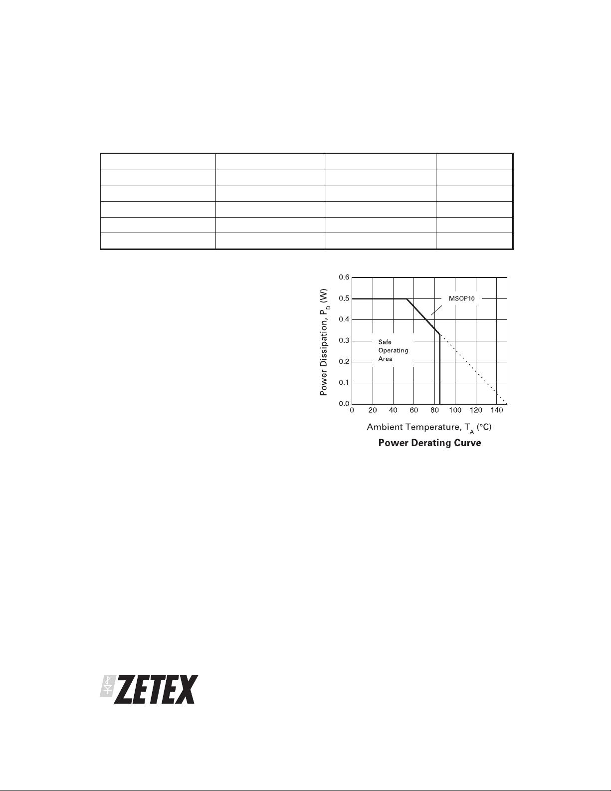
Power Dissipation
1) Maximum allowable Power Dissipation, PD,
is shown plotted against Ambient Temperature,
T
, in the accompanying Power Derating Curve,
A
indicating the Safe Operating Area for the device.
CCmax
CCmax
Dmax
OPR
STG
-0.6 to 20 V
200 mA
500 mW
-40 to 85 ⬚C
-55 to 150 ⬚C
2)Power consumed by the device, P
, can be
T
calculated from the equation:
P
= PQ+ P
T
Ph
where PQis power dissipated under quiescent
current conditions, given by:
P
= VCCx I
Q
CC
where VCCis the application
device Supply Voltage
and I
is the maximum Supply
CC
Current given in the Electrical
Characteristics
and P
is power generated due to either one of
Ph
the phase outputs Ph1 or Ph2 being
active, given by:
P
= IOLx V
Ph
OL
where IOLis the application Ph1 and Ph2
output currents
and V
is the maximum Low Level
OL
Output Voltage for the Ph1 and
Ph2 outputs given in the Electrical
Characteristics
SEMICONDUCTORS
ISSUE 4 - OCTOBER 2004
2
Page 3
ZXBM2001
ZXBM2002 ZXBM2003
Electrical Characteristics (at T
= 25°C & VCC= 12V)
amb
Parameter Symbol Min Typ Max Unit Conditions
Supply Voltage V
Supply Current I
CC
CC
4.5 18 V
2.2 3.25 mA No Load
Hall Amp Input Voltage 40 mV diff p-p
Hall Amp Common Mode Voltage V
Hall Amp Input Offset V
Hall Amp Bias Current V
PH1, PH2 Output High V
PH1, PH2 Output Off Leakage
Current
PH1, PH2 Output Current High I
Lock/FG Maximum Collector
Voltage
Lock/FG Sink Current I
Lock/FG Low Level O/P Voltage V
C
Charge Current I
LCK
C
Discharge Current I
LCK
CM
OFS
BS
OH
I
OFF
OH
V
OH
OL
OL
LCKC
LCKD
0.5 0.5V
CC
VCC-1.5 V
±7 mV
-350 nA
VCC-2.2 VCC-1.8 V IOH= 80mA
⫾10 A
-80 mA
V
CC
V
5mA
0.3 0.5 V IOL= 5mA
-1.8 -2.8 AVin= 1.5V
0.28 0.35 AVin= 1.5V
Lock condition On:Off ratio 1:7 1:10
C
High Threshold Voltage V
LCK
C
Low Threshold Voltage V
LCK
C
Charge Current I
PWM
C
Discharge Current I
PWM
PWM Frequency F
C
High Threshold Voltage V
PWM
C
Low Threshold Voltage V
PWM
SPD Voltage Control Range V
THH
THL
PWMC
PWMD
PWM
THH
THL
SPD
3.6 4.3 5.0 AVin= 1.5V
50 62 75 AVin= 1.5V
12V2
2.0 V
1.0 V
24
34
kHz
kHz
2.0 V
1.0 V
C
C
PWM
PWM
SPD Open Circuit Voltage 1.5 V 3
1
= 150pF
= 100pF
Notes:
1
Measured with pins H+, H-, C
2
The 1V minimum represents 100% PWM drive and 2V represents 0% PWM drive.
3
This voltage is determined by an internal resistor network of 52.5k⍀ from the pin to Gnd and 19.5k⍀ from the pin to a 2V reference. Whilst both
resistors track each other the absolute values are subject to a ±20% manufacturing tolerance
LCK
and C
= 0V and all other signal pins open circuit.
PWM
ISSUE 4 - OCTOBER 2004
3
SEMICONDUCTORS
Page 4

ZXBM2001
ZXBM2002 ZXBM2003
Block Diagram (ZXBM2001):
Pin Assignments
Top View
Pin Functional Descriptions
1. VCC - Applied voltage
Thisisthedevice supplyvoltage. For5V to12V fansthis
canbe supplieddirectly fromthe Fan Motorsupply. For
fans likely to run in excess of the 18V maximum rating
for the device this will be supplied from an external
regulator such as a zener diode.
SEMICONDUCTORS
2. H+ - Hall input
3. H- - Hall input
Therotor positionof the FanMotor isdetected by aHall
sensor whose output is applied to these pins. This
sensor can be either a 4 pin ‘naked’ Hall device or a 3
pin buffered switching type. For a 4 pin device the
differential Hall output signal is connected to the H+
and H- pins. For a 3 pin buffered Hall sensor the Hall
deviceoutput is attached to the H+ pin whilstthe H- pin
has an external potential divider attached to hold the
pin at half V
the active drive.
4
. When H+ is high in relation to H- Ph2 is
CC
ISSUE 4 - OCTOBER 2004
Page 5

ZXBM2001
ZXBM2002 ZXBM2003
4. SPD - Speed control voltage input
This pin provides control over the Fan Motor speed by
varying the Pulse Width Modulated (PWM) drive ratio
atthe Ph1 and Ph2 outputs.Thiscontrol signal can take
the form of either a voltage input of nominal range 2V
to 1V, representing 0% to 100% drive respectively, or
alternatively a thermistor can be attached to this pin to
control the voltage. A third method of speed control is
available by the application of an externally derived
PWM signal and this will be discussed under the C
PWM
pin.
This pin has an internal potential divider between an
internal 2.0V reference and Gnd (see Block Diagram)
designed to hold the pin at approximately 1.5V. This
will represent a drive of nominally 50% PWM. For
thermal speed control a 100k NTC thermistor is
connected between the SPD and ground will provide a
drive nominally 70% at 25°C and 100% at 50°C. As the
thermistor is connected in parallel with the internal
resistor the non-linearity of an NTC thermistor is
largely taken out. A linearity of typically ±2.5% is
achievable.
Lower values of thermistor can be used if needed and
in this situation an external potential divider will be
neededto setthe speedrange. Thiswill takethe formof
a resistor from the SPD pint to Vcc and a resistor from
the SPD pin to Gnd. Full details are given in the
ZXBM200x series Application Note.
If speed control is not required this pin is can be left
open circuit for 50% drive or tied to ground by a 10k⍀
resistor to provide 100% drive.
If required this pin can also be used as an enable pin.
The application of a voltage of 2.0V to V
will to force
CC
the PWM drive fully off, in effect disabling the drive.
5. GND - Ground
This is the device supply ground return pin and will
generally be the most negative supply pin to the fan.
6. LOCK/FG - Locked Rotor error output /
Frequency Generator (speed) output
This pin is an open collector output and so will require
an external pull up resistor for correct operation.
On the ZXBM2001 the Lock/FG pin is designed to be a
dual function pin to provide an indication of the Fans
rotational speed together with an indication of when
the Fan has failed rotating for whatever reason (Rotor
Lockedcondition). Under correct operatingconditions,
and with the external pull-up in place, this pin will
providean output signalwhose frequencywillbe twice
that of the rotational frequency of the fan. Should the
fan itself stop rotating for any reason, i.e. an
obstruction in the fan blade or a seized bearing, then
the device will enter a Rotor Locked condition. In this
condition the Lock/FG pin will go high (regardless of
the state of the Hall sensor) when the C
the V
threshold and will remain high until the fan
THH
pin reaches
LCK
blades start rotating again.
On the ZXBM2002 variant this pin is Lock. During
normal operation the signal will be low and during a
Locked Rotor condition the pin will go high when the
C
pin reaches the V
LCK
threshold.
THH
Forthe ZXBM2003 variantthispin is FG.This signal is a
buffered and inverted output of the Hall signal and
therefore provides an output signal whose frequency
willbetwicethatof therotational frequencyof thefan.
7. C
- Locked Rotor timing capacitor
LCK
When in a Locked Rotor condition as described above
thePh1 andPh2 driveoutputs gointo asafe drivemode
to protect the external drive devices and the motor
windings. This condition consists of driving the motor
for a short period then waiting for a longer period
before trying again. The frequency at which this takes
place is determined by the size of the capacitor applied
to this CLCK pin. For a 12V supply a value of 1.0uF will
typically provide an ‘On’ (drive) period of 0.33s and an
‘Off’(wait)periodof4.0s, givingan On:Offratio of1:12.
The C
timing periods are determined by the
LCK
following equations:
THH LCK
VC
lock
T
Where V
×
=
LCKC
I
THH
voltages and I
THH THL LCK
VVC
on
T
=
and V
THL
and I
LCKC
−×()
LCKC
I
are the C
LCKD
THH THL LCK
VVC
off
T
−×()
=
pin threshold
LCK
I
LCKD
are the charge and
discharge currents.
ISSUE 4 - OCTOBER 2004
5
SEMICONDUCTORS
Page 6

ZXBM2001
ZXBM2002 ZXBM2003
Locked Rotor timing capacitor (CONT).
As these threshold voltages are nominally set to
V
THH
=2V and V
=1V the equations can be simplified
THL
as follows:
8. C
T
PWM
LCK
C
×2
lock
=
LCKC
I
- Sets PWM frequency
- external PWM input
T=
on
C
I
LCK
LCKC
LCK
C
off
T
=
LCKD
I
This pin has an external capacitor attached to set the
PWM frequency for the Phase drive outputs. A
capacitor value of 0.15nF will provide a PWM
frequency of typically 24kHz.
The C
timing period (T
LCK
) is determined by the
pwm
following equation:
Where T
THH THL
(V - V ) CI(V V ) C
T=
lock
is in s
PWM
×
PWMC
+
THH THL
−×
PWMD
I
C
C
I
The C
T
PWM
=+
PWMC PWMD
I
pin can also be used as in input for an
PWM
externally derived PWM signal to control the motor
speed. The signal should have a VOL <1V and a VOH
>2V. A standard TTL or CMOS digital signal is ideal.
When driving from an external PWM source no
capacitor should be attached to the C
PWM
pin and the
SPD pin should be left open circuit.
9. PH2 - External transistor driver
10. PH1 - External transistor driver
These are the Phase drive outputs and are open
darlington emitter followers designed to provide up to
80mA of drive to external transistors as shown in the
Application circuits following. The external transistors
in turn drive the fan motor windings.
C = C
I
PWM&IPWMD
Where V
THH
voltages and I
PWM
and V
PWMC
+15 in pF
are in A
are the C
THL
and I
PWM
are the charge and
PWMD
pin threshold
discharge currents.
As these threshold voltages are nominally set to
V
=2V and V
THH
=1V the equations can be simplified
THL
as follows:
SEMICONDUCTORS
ISSUE 4 - OCTOBER 2004
6
Page 7
Lock & FG Timing Waveform:
Lock Timing Example:
Using the equation previously described and to be
found under the C
C
×2
lock
T
=
LCKC
I
LCK
LCK
pin description:
LCK
C
on
T
= T
LCKC
I
LCK
C
off
=
LCKD
I
ZXBM2001
ZXBM2002 ZXBM2003
Using a value of C
of I
LCKC
and I
= 1.0uF together with the values
LCK
to be found in the Electrical
LCKD
Characteristics we can derive the following timings for
operation at 12V and 25°C.
21.0F
T=
lock
×=
2.8 A
T=
on
s
0714.
×=
21.0F
2.8 A
T=
off
036.
1.0 F
0.28 A
s
= 36.
s
Figure 2
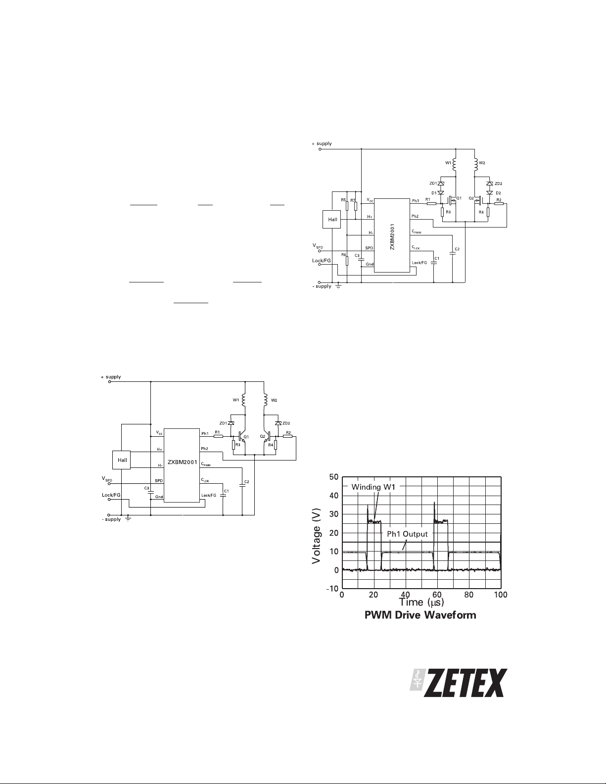
TYPICAL APPLICATION (ZXBM2001) using MOSFET power transistors
Figure 1
TYPICAL APPLICATION (ZXBM2001) using Bipolar power transistors
ISSUE 4 - OCTOBER 2004
Graph 1
7
SEMICONDUCTORS
Page 8

ZXBM2001
ZXBM2002 ZXBM2003
APPLICATION INFORMATION
Thissection givesa briefinsight intoapplications using
the ZXBM200x series. More complete data is available
in the ZXBM200x Series Applications Note, visit
www.zetex.com/zxbm or contact your nearest Zetex
office for full details.
The ZXBM200x series of 2-phase DC brushless motor
pre-drivers are capable of driving both Bipolar or
MOSFET power transistors.
For smaller fans and blowers it is likely that bipolar
power transistors would be used as shown in the
following Applications circuit.
InFigure 1,R1 & R2have theirvalue selected toprovide
suitable base current in keeping with the winding
currentand gainof the powertransistors Q1& Q2. R3&
R4 have their value selected to provide efficient
switch-off of Q1 & Q2. The Zener diodes ZD1 & ZD2
provideactiveclampinginconjunction withQ1 &Q2.
It is also recommended that the supply de-coupling
capacitor C3 is positioned as close as is practical to the
ZXBM device pins.
In the case of higher power fans and blowers it may be
more applicable to use MOSFET devices to switch the
windings as illustrated in the second applications
circuit shown in Figure 2.
In Figure 2, the Resistor ratio of R1 to R3 and R2 to R4
provide the required Gate turn-on voltage whilst the
absolute values will be chosen to provide sufficient
gate switching currents.
Also illustrated in the two Applications circuits above
are the methods of connection for both a ‘naked’ Hall
device, as seen in the bipolar circuit in Figure 1, and a
bufferedHall device, as in the MOSFET circuitin Figure
2.In thislatter circuitR5 &R6 biasthe H-pin atavoltage
equivalent to half the swing of the Hall device. R7 will
be needed if the buffered Hall device does not have its
own internal pull-up.
Graph 1 below, illustrates the PWM drive waveform
takenfrom and applicationusing theMOSFETcircuit in
Figure 2. This shows the waveforms to be found at the
Ph1 output and at the drain/Winding node.
SEMICONDUCTORS
ISSUE 4 - OCTOBER 2004
8
Page 9

ZXBM2001
ZXBM2002 ZXBM2003
When driving fans with bipolar transistors, at higher
voltages it may be necessary to provide extra noise
protection by the addition of a diode from the driver
collectorto Gnd on each phase. This prevents negative
voltage excursions from the windings affecting
operation. See Figure 3 right, showing the placement
of these diodes. It should be noted that these are not
required for the MOSFET solution in Figure 2 as the
diodes are inherent in the MOSFET structure.
Zetexprovide avariety ofsuitable powertransistors for
using with the ZXBM200x series of 2-phase DC
brushless motor pre-drivers and suitable devices
sufficient for a range of applications are given in the
following table.
Figure 3
TYPICAL APPLICATION (ZXBM2001) illustrating addition of Clamp
diodes.
SUMMARY TABLE OF SUITABLE DEVICES
Bipolar Types V
FZT1053A 75 4.5 300 @ 0.5A 200 @ 1A, 10mA SOT223
FZT851 60 6 100 @ 2A 100 @ 1A, 10mA SOT223
FZT853 100 6 100 @ 2A 175 @ 1A, 100mA SOT223
FZT855 150 4 100 @ 1A 65 @ 0.5A, 50mA SOT223
ZXT13N50DE6 50 4 300 @ 1A 100 @ 1A, 10mA SOT23-6
(V) IC(A) min HFE@ICV
CEO
CE(sat)
@I
max(mV)
C&IB
Package
MOSFET Types BV
ZXMN3A04DN8
ZXMN6A09DN8
ZXMN6A11Z
ZXMN6A11G 60 3.8 10 140 @ 10V SOT223
ZXMN10A11G
Notes:
1
Contact your nearest Zetex office for further details and technical enquiries.
2
Dual device
3
Provisional information
4
Advanced information
23
23
1
24
(V) ID(A) I
DSS
(A)
PEAK
(Pulsed)
R
DS(on)
max(m )
@V
GS
30 7.6 25 20 @ 10V SO8
60 5 17.6 45 @ 10V SO8
60 3.8 10 140 @ 10V SOT89
100 1.9 5.9 600 @ 10V SOT223
ISSUE 4 - OCTOBER 2004
9
SEMICONDUCTORS
Package
Page 10

ZXBM2001
ZXBM2002 ZXBM2003
Conforms to JEDEC MO-187 VARIATION BA
CONTROLING DIMENSIONS IN METRIC
APPROX. DIMENSION IN INCHES
PACKAGE DIMENSIONSPACKAGE OUTLINE
MILLIMETERS INCHES
DIM
MIN. MAX. MIN. MAX.
A ᎏ 1.10 ᎏ 0.43
A1 ᎏ 0.15 ᎏ 0.006
A2 0.75 0.95 0.0295 0.037
D 3.00 BSC 0.118 BSC
E 4.90 BSC 0.1929 BSC
E1 3.00 BSC 0.118 BSC
b 0.17 0.27 0.0066 0.0106
c 0.08 0.23 0.003 0.009
e 0.50 BSC 0.0196 BSC
⍜ 0⬚ 15⬚ 0⬚ 15⬚
L 0.40 0.80 0.015 0.031
L1 0.95 BSC 0.037 BSC
© Zetex Semiconductors plc 2004
Europe
Zetex GmbH
Streitfeldstraße 19
D-81673 München
Germany
Telefon: (49) 89 45 49 49 0
Fax: (49) 89 45 49 49 49
europe.sales@zetex.com
These offices are supported by agents and distributors in major countries world-wide.
Thispublicationis issued to provide outline informationonlywhich (unless agreed by the Companyinwriting) may not be used, appliedorreproduced
for any purpose or form part of any order or contract or be regarded as a representation relating to the products or services concerned. The Company
reserves the right to alter without notice the specification, design, price or conditions of supply of any product or service.
For the latest product information, log on to www.zetex.com
Americas
Zetex Inc
700 Veterans Memorial Hwy
Hauppauge, NY 11788
USA
Telephone: (1) 631 360 2222
Fax: (1) 631 360 8222
usa.sales@zetex.com
Asia Pacific
Zetex (Asia) Ltd
3701-04 Metroplaza Tower 1
Hing Fong Road, Kwai Fong
Hong Kong
Telephone: (852) 26100 611
Fax: (852) 24250 494
asia.sales@zetex.com
Corporate Headquaters
Zetex Semiconductors plc
Lansdowne Road, Chadderton
Oldham, OL9 9TY
United Kingdom
Telephone (44) 161 622 4444
Fax: (44) 161 622 4446
hq@zetex.com
ISSUE 4 - OCTOBER 2004
SEMICONDUCTORS
10
 Loading...