Diodes ZXBM1016 User Manual

ZXBM1016
ZXBM1016
V
CC
H+
H-
C
PWM
C
LCK
SPD
C3C2
C1
1μF
100pF 0.47μF
0V
FG
0.1μF
ThRef
S
MIN
Ph1Lo
Ph2Lo
Gnd
C
INT
Q1-4
W1
470Ω
R2
470Ω
ZXMC
3A17DN8
FG
Ph1Hi
Ph2Hi
R1
R5
R3
R4
R6
100Ω
100Ω
1kΩ
1kΩ
C6
2.2μF
12V
D1
1N4148
D2
1N4004
SetTh
Sense
CONTROL
C4
R18
10kΩ
R15
R13
R12
R14
R17
R16
1kΩ
4.7kΩ
4.7kΩ
4.7kΩ
1kΩ
47kΩ
Q5
Q6
R10
16kΩ
R9
12kΩ
Hall
R8
470Ω
R7
33kΩ
Rsense
0.1Ω
33
44
5 & 6
5 & 6
7 & 8 7 & 8
2
2
11
Range
H-Bias
C5
0.47μF
SetThRef
R11
220kΩ
TSSOP20
High efficiency variable speed single-phase fan motor controller
Description
The ZXBM1016 is a high efficiency, low noise,
single-phase, DC brushless motor pre-driver
with PWM variable speed control and current
control suitable for fan and blower motors.
High efficiency and low noise are achieved
using a novel technique (patent pending) for
commutation current control.
The controllers are primarily intended to meet
industry standard OEM fan specifications where
external PWM control are applied, however,
they can also be used with other thermal control
techniques using an external voltage, PWM
signal or thermistor.
Features
• Compliant with external PWM speed control
• Compliant with thermistor control
• Minimum speed setting
• High efficiency utilizing tail-end current control
•Low noise
•Auto restart
• Built in Hall amplifier
• Hall bias
• Speed pulse (FG) output
• Integrated current control
• Up to 18V input voltage (60V with external regulator)
• Small TSSOP20 package
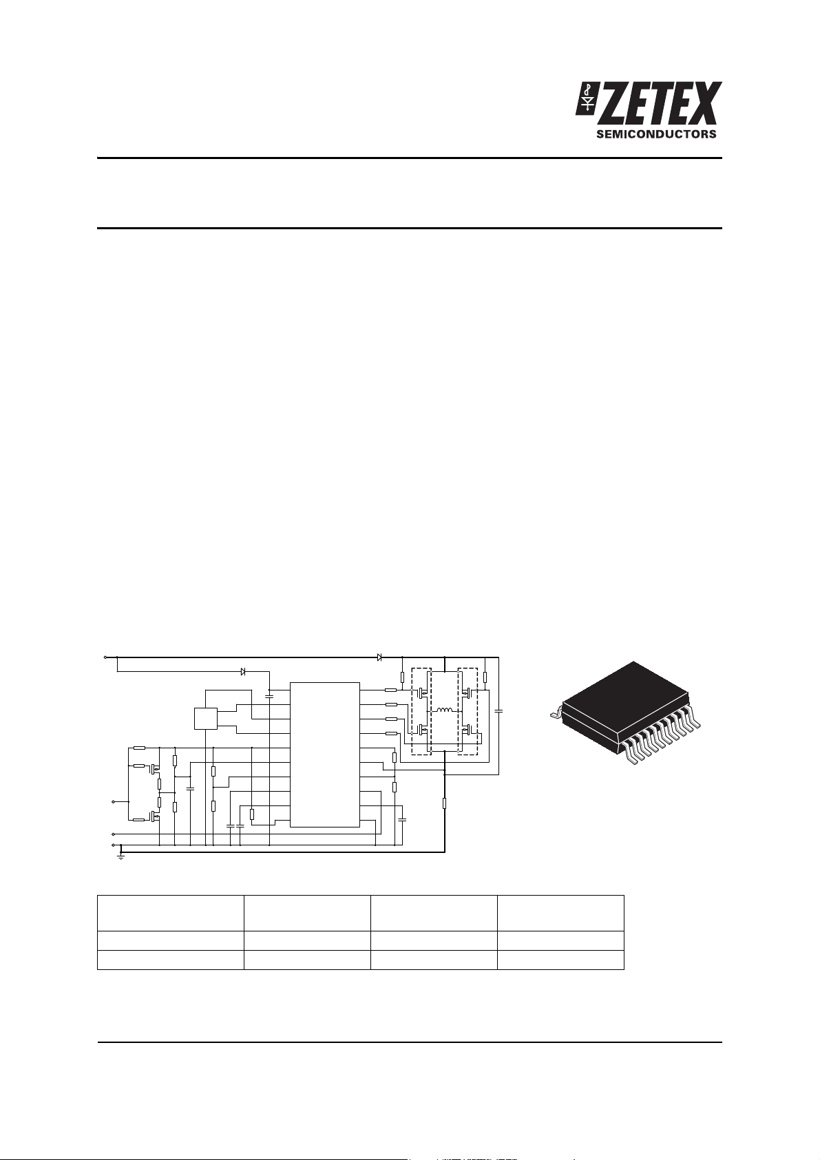
Applications circuit
Applications
• Mainframe and personal computer fans and
blowers
• Instrumentation fans
• Central heating blowers
• Automotive climate control
Ordering information - TSSOP20
Device Reel size
(inches)
ZXBM1016ST20TA 7 (180mm) 16 1000
ZXBM1016ST20TC 13 (330mm) 16 2,500
Device marking
ZETEX
ZXBM1016
Date code
Issue 1 - February 2007 1 www.zetex.com
© Zetex Semiconductors plc 2007
Tape width
(mm)
Quantity
per reel

ZXBM1016
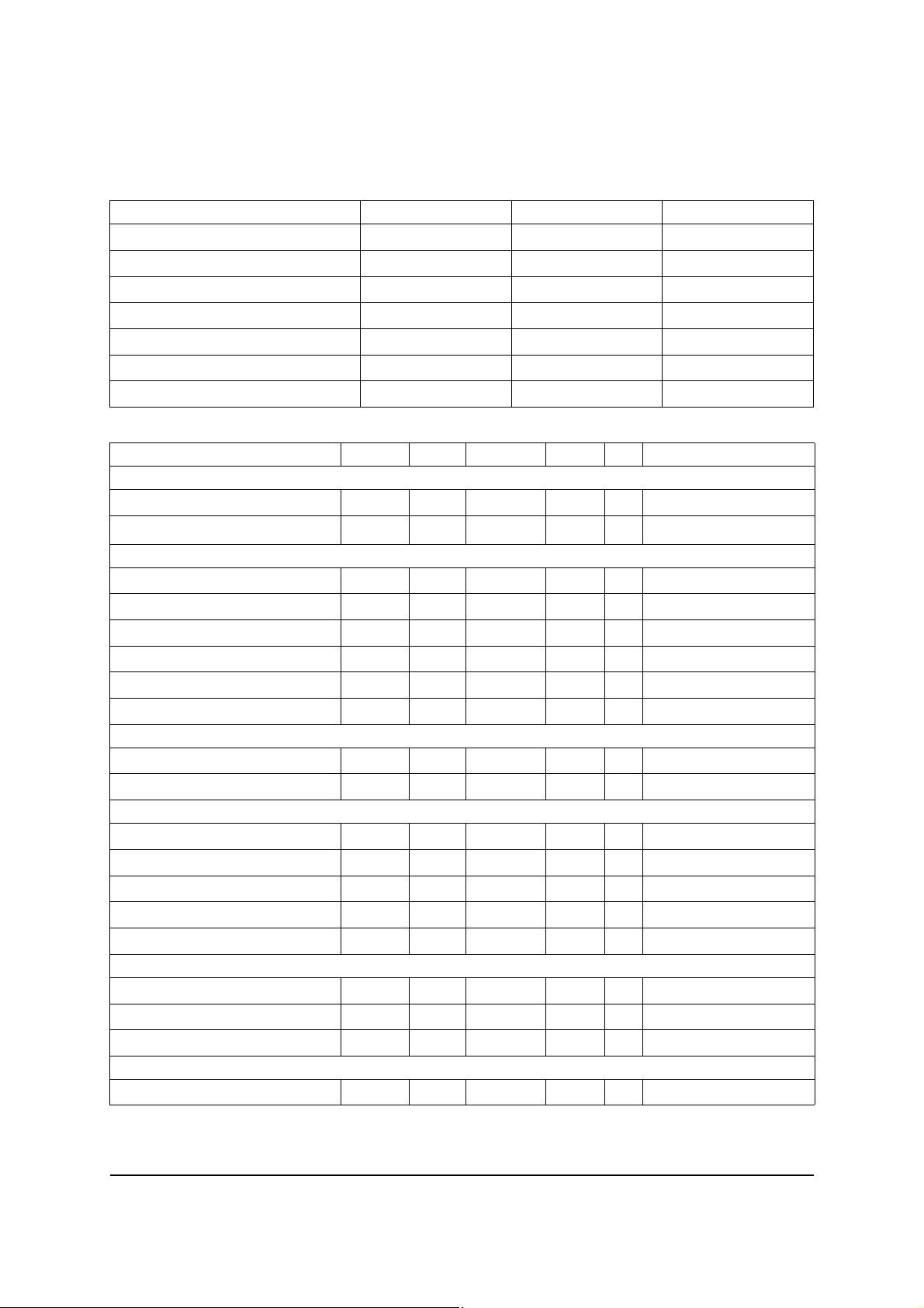
Absolute maximum ratings
Parameter Symbol Limits Unit
Supply voltage V
Input current I
Maximum input voltage V
Maximum output voltage V
Power dissipation P
Operating temperature T
Storage temperature T
CCmax
CCmax
Imax
Omax
Dmax
OPR
STG
-0.6 to 20 V
200 mA
-0.6 to VCC+0.5 V
-0.6 to VCC+0.5 V
800 mW
-40 to 85 °C
-55 to 125 °C
Electrical characteristics (at T
= 25°C and VCC = 12V unless otherwise stated)
amb
Parameter Symbol Min. Typ. Max. Unit Conditions
Supply
Supply voltage V
Supply current I
CC
CC
6.7 18 V For valid ThRef
15 20 mA
= 12V, no load
V
CC
Hall connections
Hall amp input voltage V
Hall amp common mode voltage
Hall amp input hysteresis V
Hall amp input current I
Hall bias voltage V
Hall bias output current I
V
IN
CM
OFS
BS
HB
HB
40 mV diff p-p
0.5 VCC-1.5 V
12 mV
700 1000 nA
1.5 1.75 1.95 V I
HBout
-10 mA
= -5mA
Reference voltage
ThRef voltage V
ThRef output current I
PWM oscillator
C
charge current I
PWM
discharge current I
C
PWM
high threshold voltage V
C
PWM
low threshold voltage V
C
PWM
PWM frequency F
ThRef
OThRef
PWMC
PWMD
THH
THL
PWM
4.75 5.0 5.25 V I
-10 mA
-5.3 -7 -9.2 A
50 75 100 A
3V
1
V
25 kHz C
OThRef
PWM
=-10mA
= 0.1nF
Speed control
SPD voltage minimum V
SPD voltage maximum V
SPD input current I
SPDL
SPDH
ISPD
1 V 100% PWM drive
3 V 0% PWM drive
0.8 2 AVIN = 2V
Minimum speed setting
input current I
S
MIN
ISMIN
-0.25 -0.5 AVIN = 2V
(*)
Issue 1 - February 2007 2 www.zetex.com
© Zetex Semiconductors plc 2007

ZXBM1016
NOTES:
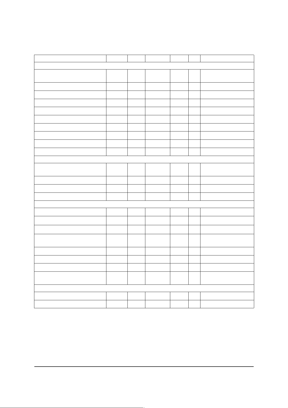
Parameter Symbol Min. Typ. Max. Unit Conditions
Tail-end current control
Range pin input current setting
range
Range pin input voltage V
charge current - lock I
C
LCK
C
charge current - run I
LCK
discharge current - lock I
C
LCK
C
high threshold voltage V
LCK
low threshold voltage V
C
LCK
input current - lock I
C
INT
C
charge current - run I
INT
discharge current - run I
C
INT
Current limit
SetThRef output voltage
SetThRef output current I
Sense input current I
SetTh input current I
Output drives
Ph1Lo, Ph2Lo output high voltage
Ph1Lo, Ph2Lo output low voltage
Ph1Lo, Ph2Lo output low voltage
Ph1Lo, Ph2Lo output source
current
Ph1Lo, Ph2Lo output sink current
Ph1Hi, Ph2Hi output low voltage
Ph1Hi, Ph2Hi output sink current
Ph1Hi, Ph2Hi off output
leakage current
Output flag
FG output current I
FG low level output voltage V
I
Range
IN
LCKCL
LCKCR
LCKDL
THH
THL
INTCL
INTCR
INTDR
V
SetThRef
SetThRef
Sense
SetTh
V
OH
V
OLA
V
OLB
I
OH
I
OL
V
OLA
I
OL
I
OFF
OL
OL
4 50A
0.50 0.65 0.75 V Input current = 20A
-0.75 -1.42 -1.8 A
-(4xI
) A Run mode
Range
0.8 0.8 1.25 A
Lock mode, V
Lock mode, V
5V
1 V Lock mode
-50 300n nA
Lock mode, V
-1 mA Run mode
ThRef-
0.5V
0.8xI
ThRef-
0.25V
Range
A Run mode
VI
SetThRef
=200A
-200 A
-20 -100 nA VIN=1V, SetTh=2V
-20 -100 nA VIN=2V, sense=1V
V
2.2
V
CC–
1.8 V IOH =80mA
CC–
0.4 0.6 V
0.4 0.6 V
I
OL
I
OL
=16mA
=50A
-80 mA
80 mA
0.5 0.75 V IOL =100mA
100 mA
±100 nA
16 mA
0.5 V IOL = 16mA
(†)
(‡)
CLCK
CLCK
CLCK
= 2.5V
= 2.5V
= 2.5V
(*) Measured with pins H+, H-, C
(†) Measured when opposing phase output is low.
(‡) Measured when opposing phase output is high.
LCK
and C
= 0V and all other signal pins open circuit.
PWM
Issue 1 - February 2007 3 www.zetex.com
© Zetex Semiconductors plc 2007

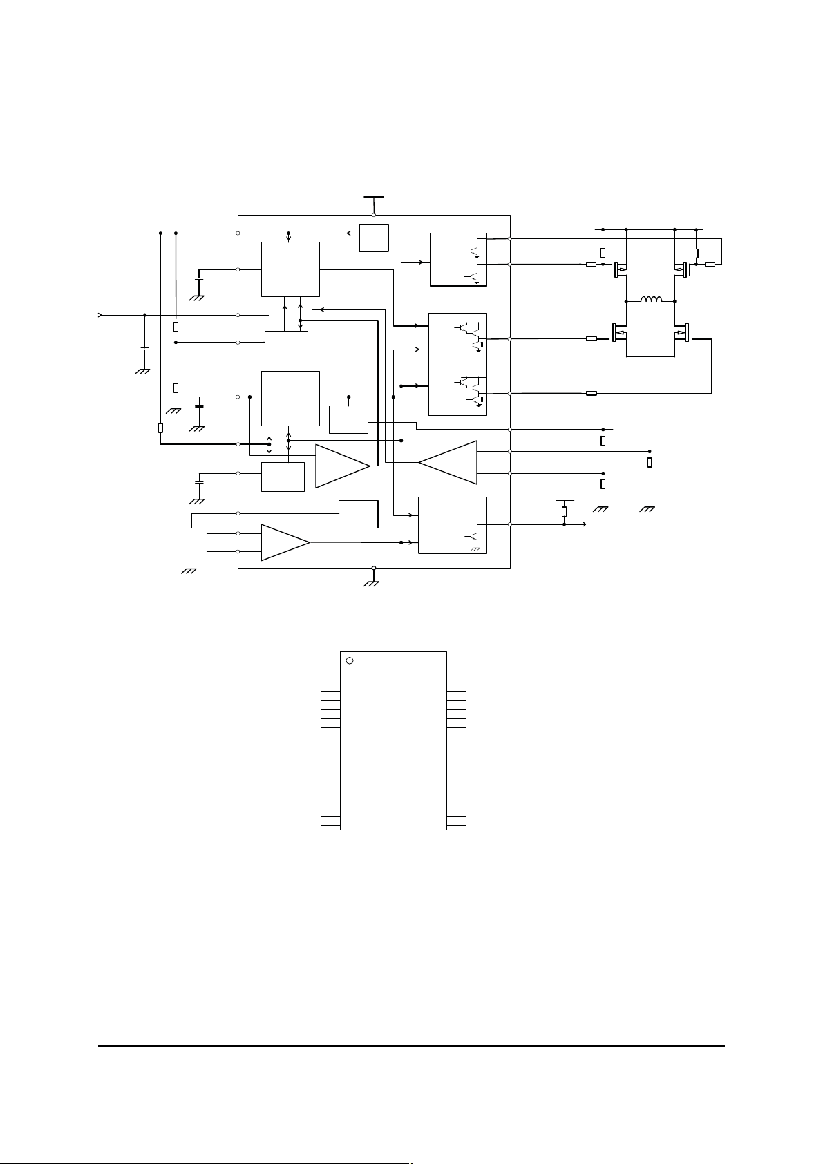
Block diagram
ThRef
CPWM
PWM
Osc
Vcc
Vref
Phase
Drive
Ph1 Hi
Ph2 Hi
ZXBM1016
Vcc
V
SPD
Control
Voltage
SPD
SMIN
CLCK
Range
CINT
H-Bias
Hall
Pin assignments
H+
Vcc
Set Min
Speed
Locked
Rotor
Detect
Speed
Detect
H-
Hall
Amp
Vcc
Start-up
Tail-end
Control
1
Hall
Bias
Gnd
Phase
Drive &
Control
Current
Monitor
Speed &
Lock
Detect
Vcc
H+
H-Bi as
H-
ThRef
SPD
S
PWM
C
C
LCK
MIN
ZXBM1016
TSSOP20
Range
Ph2Hi
Ph1Lo
Ph2Lo
Ph1Hi
SetThRef
Sense
SetTh
FG
C
INT
Gnd
Ph1 Lo
Ph2 Lo
SetThRef
Sense
SetTh
Vcc
FG
Issue 1 - February 2007 4 www.zetex.com
© Zetex Semiconductors plc 2007
 Loading...