

Page 1
SEMICONDUCTORS
ZXBM1004
VARIABLE SPEED SINGLE-PHASE BLDC MOTOR CONTROLLER
DESCRIPTION
The ZXBM1004 is a single-phase, DC brushless motor pre-driver with PWM
variable speed control suitable for fan and blower motors. The controller is
intended for applications where the fan or blower speed is controlled by an
external PWM signal, thermistor or DC voltage.
FEATURES
Compliant with external PWM speed control
•
Compliant with thermistor control
•
Minimum speed setting
•
Low noise
•
Auto restart
•
Built in hall amplifier
•
Speed pulse (FG) and lock rotor (RD) outputs
•
Up to 18V input voltage (60V with external regulator)
•
QSOP16 package
•
Q
O
1
6
P
S
Associated application notes:-
AN41 - Thermistor control
AN42 - External PWM control
AN43 - Interfacing to the motor windings
APPLICATIONS
•
Mainframe and personal computer fans and blowers
•
Instrumentation fans
•
Central heating blowers
•
Automotive climate control
ORDERING INFORMATION - QSOP16
DEVICE
ZXBM1004Q16TA
ZXBM1004Q16TC
REEL SIZE TAPE WIDTH QUANTITY PER REEL
7" (180mm)
13" (330mm)
DEVICE MARKING
•
ZETEX
ZXBM
1004
ISSUE 6 - MAY 2007
12mm
12mm
500
2,500
1
Page 2
ZXBM1004
SEMICONDUCTORS
ABSOLUTE MAXIMUM RATINGS
PARAMETER SYMBOL LIMITS UNIT
Supply voltage V
Input current I
Input voltage V
Output voltage V
Power dissipation P
Operating temp. T
Storage temp. T
CCmax
CCmax
max
IN
OUT
Dmax
OPR
STG
max
-0.6 to 20 V
200 mA
-0.5 to V
-0.5 to V
-40 to 110 ⬚C
-55 to 150 ⬚C
+0.5 V
CC
+0.5 V
CC
500 mW
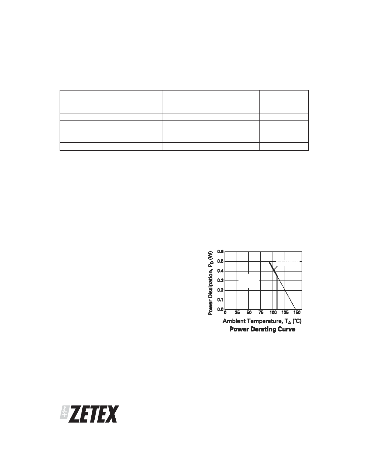
Power Dissipation
1) Maximum allowable Power Dissipation, PD,
is shown plotted against Ambient Temperature,
T
, in the accompanying Power Derating Curve,
A
indicating the Safe Operating Area for the device.
2) Power consumed by the device, P
calculated from the equation:
P
= PQ+ P
T
where PQis power dissipated under quiescent
and P
+ P
PhHi
PhLo
current conditions, given by:
P
= Vcc x Icc
Q
where Vcc is the application
device Supply Voltage
and Icc is the maximum Supply
Current given in the Electrical
Characteristics
is power generated due to eitheroneof
PhHi
the phase outputs Ph1Hi or Ph2Hi being
active, given by:
P
= IOLx V
PhHi
where IOLis the application Ph1Hi and Ph2Hi
and V
OL
output currents
is the maximum Low Level
OL
Output Voltage for the Ph1Hi and
Ph2Hi outputs given in the Electrical
Characteristics
, can be
T
and P
is power generated due to eitheroneof
PhLo
the phase outputs Ph1Lo or Ph2Lo being
active, given by:
P
= IOHx (VCC- VOH)
PhLo
where I
is the application Ph1Lo andPh2Lo
OH
output currents
and Vcc is the application device Supply
Voltage
and V
is the minimum High Level
OH
Output Voltage for the Ph1Lo and
Ph2Lo outputs given in the Electrical
Characteristics
ISSUE 6 - MAY 2007
2
Page 3
ZXBM1004
SEMICONDUCTORS
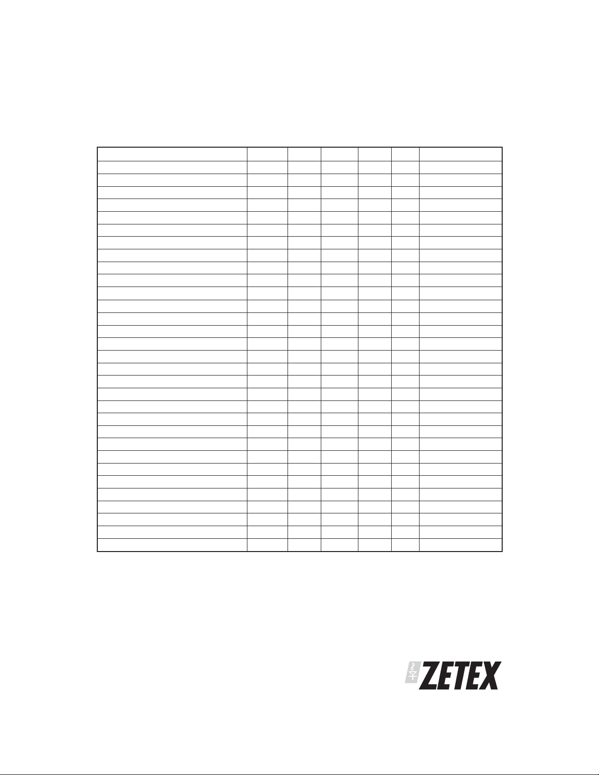
ELECTRICAL CHARACTERISTICS (at T
amb
PARAMETER SYMBOL
Supply voltage V
Supply current I
Hall amp input voltage V
Hall amp common mode voltage V
Hall amp input offset V
Hall amp bias current I
Ph1Lo, Ph2Lo output high voltage
Ph1Lo, Ph2Lo output low voltage
Ph1Lo, Ph2Lo output low voltage
Ph1Lo, Ph2Lo output source current
Ph1Lo, Ph2Lo output sink current
Ph1Hi, Ph2Hi output low voltage
Ph1Hi, Ph2Hi output sink current
C
charge current
PWM
discharge current I
C
PWM
high threshold voltage V
C
PWM
low threshold voltage V
C
PWM
PWM frequency F
ThRef voltage V
ThRef output current I
input current I
S
MIN
SPD voltage minimum V
SPD voltage maximum V
SPD input current I
C
charge current I
LCK
discharge current I
C
LCK
high threshold voltage V
C
LCK
low threshold voltage V
C
LCK
CC
CC
IN
CM
OFS
BS
V
OH
V
OLA
V
OLB
I
OH
I
OL
V
OL
I
OL
I
PWMC
PWMD
THH
THL
PWM
ThRef
OThRef
ISMIN
SPDL
SPDH
ISPD
LCKC
LCKD
THH
THL
Lock condition On:Off ratio
FG & RD output current I
FG & RD low level output voltage V
OL
OL
= 25°C & VCC= 12V)
MIN. TYP. MAX. UNIT
4.7 18 V
6 8.5 mA No load
40 mV diff p-p
0.5 VCC-1.5 V
⫾7mV
400 650 nA
VCC-2.2 VCC-1.8 V IOH=80mA
0.4 0.6 V IOL=16mA
0.4 0.6 V IOL=50A
-80 mA
16 mA
0.5 0.7 V
100 mA
-6.2 -7.6 -9 A
65 80 95 A
2.9533.15V
0.9411.11V
24 kHz
2.925 3.0 3.14 V
-0.2 -1 mA
-0.25 -0.5 A
1V
3V
-0.8 -2 A
-2 -3 A
0.2 0.35 A
3V
1V
1:12
5mA
0.5 V
CONDITIONS
I
=100mA
OL
C
PWM
I
OThRef
Vin = 2V
100% PWM drive
0% PWM drive
Vin = 2V
I
=5mA
OI
(1)
(2)
(3)
=0.1nF
=-100A
Notes:
(1) Measured with pins H+, H-, C
(2) Measured when opposing phase output is low.
(3) Measured when opposing phase output is high.
and C
LCK
= 0V and all other signal pins open circuit.
PWM
ISSUE 6 - MAY 2007
3
Page 4
ZXBM1004
SEMICONDUCTORS
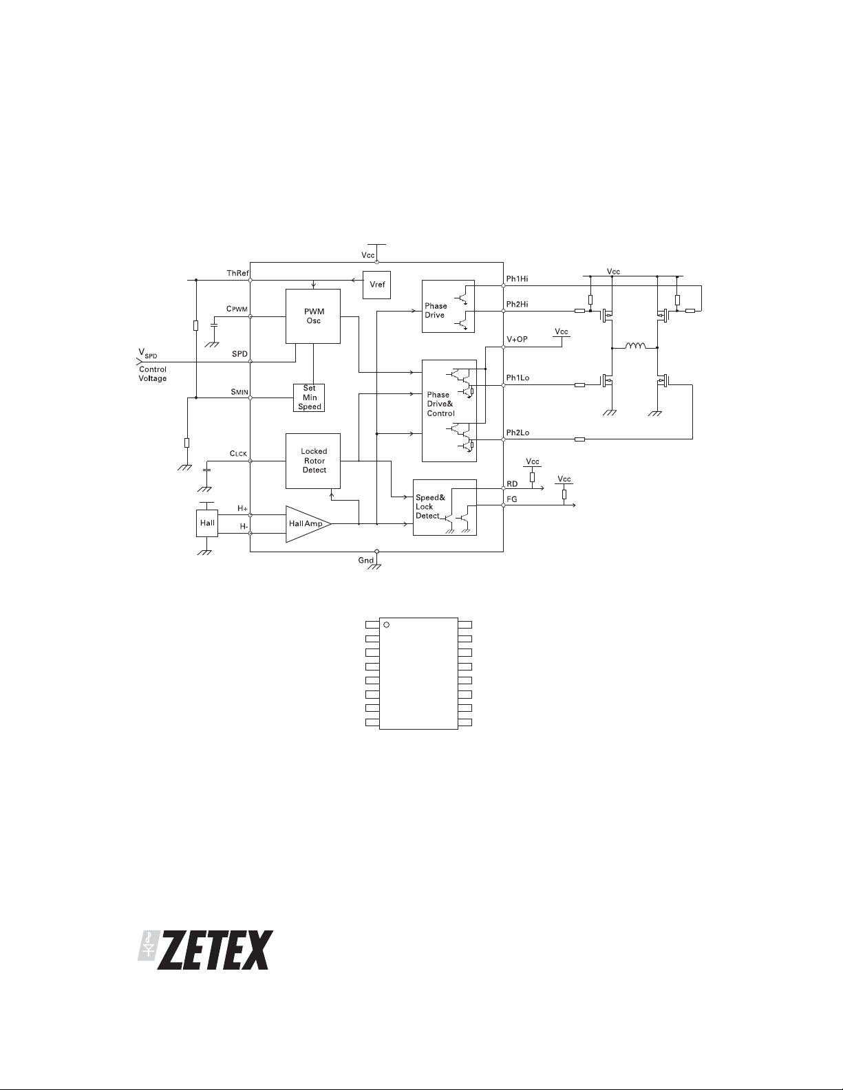
Vcc
SPD
H+
H-
Gnd
Ph1Lo
Ph2Lo
C
PWM
CLCK
FG
ZXBM1004
QSOP16
RD
V+OP
ThRef
S
MIN
1
Ph1Hi
Ph2Hi
Block diagram
Pin assignments
ISSUE 6 - MAY 2007
4
Page 5

ZXBM1004
SEMICONDUCTORS
PIN FUNCTIONAL DESCRIPTION
H+ - Hall input
H- - Hall input
The rotor position is detected by a Hall sensor, with the
output applied to the H+ and H-pins. Thissensor can be
either a 4 pin 'naked' Hall device or of the 3 pin buffered
switching type. For a 4 pin device the differential Hall
output signal is connected to the H+ and H- pins. For a
buffered Hall sensor the Hall device output is attached
to the H+ pin, with a pull-up attached if needed, whilst
the H- pin has an external potential divider attached to
hold the pin at halfV
Ph2 is the active drive.
. When H+ is highin relation to H-,
cc
ThRef - Network Reference
This is a reference voltage of nominal 3V. It is designed
for the ability to 'source' and therefore it will not 'sink'
any current from a higher voltage.
The total current drawn from the pin by the minimum
speed potential divider to pin S
setting network should not exceed 1mA at maximum
temperature.
and any voltage
MIN
SPD - Speed Control Input
The voltage applied to the SPD pin provides control
over the Fan Motor speed by varying the Pulse Width
Modulated (PWM) drive ratio at the Ph1Lo and Ph2Lo
outputs. The control signal takes the form of a voltage
input of range 3V to 1V, representing 0% to 100% drive
respectively.
If variable speed control is not required this pin can be
left with an external potential divider to set a fixed
speed or tied to ground to provide full speed i.e. 100%
PWM drive.
If required this pin can also be used as an enable pin.
The application of a voltage >3.0V will force the PWM
drive fully off, in effect disabling the drive.
S
- Sets Minimum Speed
MIN
A voltage can be set on this pin via a potential divider
between the ThRef and Gnd. This voltage is monitored
by the SPD pin such that it cannot rise above it. As a
higher voltage on the SPD pin representsa lower speed
it therefore restricts the lower speed range of the fan. If
this feature is not required the pin is lefttied to ThRef so
no minimum speed will be set.
If the fan is being controlled from an external voltage
source onto the SPD pin then either this feature should
not be used or if it is required then a >1k⍀ resistor
should be placed in series with the SPD pin.
C
- Sets PWM Frequency
PWM
This pin has an external capacitor attached to set the
PWM frequency for the Phase drive outputs. A
capacitor value of 0.1nF will provide a PWM frequency
of typically 24kHz.
The C
following equation:
T
PWM
Where: C = C
timing period (T
PWM
VVxCIVVxC
−
THH THL
=
PWMC
+15, in pF
PWM
V
and V
THH
threshold voltages
I
and I
PWMC
discharge currents in A.
T
PWM
PWMD
is in ms
) is determined by the
PWM
−()()
THH THL
+
I
PWMD
are the C
THL
are the charge and
PWM
pin
ISSUE 6 - MAY 2007
5
Page 6

ZXBM1004
SEMICONDUCTORS
As thesethreshold voltages are nominally set to V
3V and V
follows:
T
=+
PWM
C
LCK
Should the fan stop rotating for any reason, i.e. an
obstruction in the fan blade or a seized bearing, then
the device will enter a Rotor Locked condition. In this
condition after a predetermined time (T
will go high and the Phase outputs will be disabled.
After a further delay (T
the Phasedrive for a defined period (T
to re-start the fan. This cycle of (T
repeated indefinitely or until the fan re-starts.
= 1V the equations can be simplified as
THL
C
22
I
PWMC PWMD
C
I
- Locked rotor timing capacitor
LOCK
) the controller will re-enable
OFF
) in an attempt
ON
) and (TON) will be
OFF
THH
) the RD pin
GND - Ground
This is the device supply ground return pin and will
generally be the most negative supply pin to the fan.
RD - Locked Rotor error output
This pin is the Locked Rotor output as referred to in the
C
timing section above. It is high when the rotor is
LCK
stopped and low when it is running.
This is an open collector drive giving an active pull
down withthe high level being provided by an external
pull up resistor.
FG - Frequency Generator (speed) output
This is the Frequency Generator output and is a
buffered signal from the Hall sensor.
Ph1Lo & Ph2Lo - Low-side External
=
H-bridge Driver
This pair of outputs drive the Low side of the external
high power H-bridge devices which in turn drives the
single phase winding. These outputs provide both the
commutation and PWM waveforms. The outputs are of
the Darlington emitter follower type with an active
pull-down to help faster switch off when using bipolar
devices. When in the high state the outputswill provide
up to 80mA of drive into the base or gates of external
transistors as shown in the Typical Application circuit
following.
When in the low state the active Phase drive is capable
of sinking up to 16mA when driving low to aid turn off
times during PWM operation. When the Phase is
inactive the output is held low by an internal pull-down
resistor.
Ph1Hi & Ph2Hi - High-side External H-bridge
Driver
These are the High side outputs to the external
H-bridge and are open collector outputs capable of
sinking 100mA. This signal provides commutation only
to the H-bridge.
V+OP - Phase Outputs Supply Voltage
This pin is the supply to the Phase outputs and will be
connected differently dependant upon external
transistor type.
For bipolar devices this pin will be connected by a
resistor to the V
the current into the transistor base so its value is
chosen accordingly.
For MOSFET devices the pin will connect directly to the
V
pin.
CC
pin. The resistor is used to control
CC
This is an open collector drive giving an active pull
down withthe high level being provided by an external
pull up resistor.
ISSUE 6 - MAY 2007
6
Page 7

VCC- Applied Voltage
SEMICONDUCTORS
TLock
TOff
TOn
Hall
C
LCK
FG
RD
VTHH
VTHL
This is the device internal circuitry supply voltage. For
5V to 12V fans thiscan be supplied directly fromthe Fan
Motor supply. For fans likely to run in excess of the 18V
maximum rating for the device this will be supplied
from an external regulator such as a Zener diode.
RD Timing Waveform:
ZXBM1004
Applications Information
The ZXBM1004 is primarily controlled by a voltage on
the SPD pin. A voltage of 1V represents a 100% PWM at
the Phase Outputs and in turn represents full speed. 3V
on the SPD pin conversely represents 0% PWM. The
motor cantherefore be controlled simply by applying a
control voltage onto the SPD pin with the minimal use
of external components.
This voltage control method easily lends itself to
control by other signal types. For example if a
thermistor is applied to the SPD pin a varying voltage
can be generated at the SPD pin as the resistance of the
thermistor varies with temperature.
ISSUE 6 - MAY 2007
A common form of control of fans is by a PWM signal
derived from a central processor or controller. This
signal can be converted into a voltage and that voltage
adjusted as neccesary to compensate for motor none
linearity, inclusion of the Minimum speed feature etc.
Full applications details and furtherexamples of how to
control the ZXBM1004 are available in the Applications
Notes AN41, AN42 and AN43.
7
Page 8

ZXBM1004
SEMICONDUCTORS
Figure 1: Typical circuit for thermistor controlled speed
Figure 2: Typical circuit for external PWM controlled speed
ISSUE 6 - MAY 2007
8
Page 9

SEMICONDUCTORS
Figure 3: Typical circuit for 48V input and external PWM control
ZXBM1004
Figure 4: Typical circuit for constant speed operation
ISSUE 6 - MAY 2007
9
Page 10

ZXBM1004
SEMICONDUCTORS
Drive transisitors
Zetex offersa range of devices that are ideally suited to
interface between the ZXBM1004 controller and the
motor. The following tables show a selection of
products ranging from single packaged H-bridge
devices to individual power components that can be
used in this application. If your needs are not covered
by this selection then please refer to the the more
comprehensive listings that can be found on the Zetex
website: www.zetex.com
Description
MOSFET
Part Number
ZXMHC6A07T8
H-Bridge
ZXMHC3A01T8
N+P
ZXMC4559DN8
channel
MOSFET
Low side
switch
MOSFET
ZXMC3A16DN8
ZXMN10A09K
ZXMN6A09K
ZXMN3A04K
Description Part Number
High side
switch
Bipolar
ZXT953K
ZXT951K
ZXT790AK
Content BV
2 x N
2 x P
2 x N
2 x P
N
P
N
P
N
N
N
Content BV
PNP
PNP
PNP
DSS
V
60
-60
30
-30
60
-60
30
-30
100
60
30
CEO
V
-100
-60
-40
I
D
A
1.8
-1.5
3.1
-2.3
4.7
-3.5
6.4
-5.4
7.7
11.2
18.4
I
A
-5
-6
-3
I
DM
A
8.7
-7.5
14.5
-10.8
22
-18
30
-25
27
40
66
C
I
CM
A
-10
-15
-6
R
DS(on)
V
@ VGS=10V
max. m
300
425
120
210
55
105
35
48
85
45
20
at IC=2A
CE(sat)
max. mV
-175
-165
-450
Package
SM-8
SM-8
SO8
SO8
DPAK
Package
DPAK
ISSUE 6 - MAY 2007
10
Page 11

ZXBM1004
SEMICONDUCTORS
Definitions
Product change
Zetex Semiconductors reserves the right to alter, without notice, specifications, design, price or conditions of supply of any product or service.
Customers are solely responsible for obtaining the latest relevant information before placing orders.
Applications disclaimer
The circuitsin this design/application noteare offered as designideas. It is theresponsibility of the userto ensure that thecircuit is fit forthe user's
application andmeets with theuser's requirements. Norepresentation orwarranty is givenand noliability whatsoever isassumed byZetex with
respect to the accuracy or use of such information, or infringement of patents or other intellectual property rights arising from such use or
otherwise. Zetex does not assume any legal responsibility or will not be held legally liable (whether in contract, tort (including negligence),
breach ofstatutory duty, restriction or otherwise)for any damages, loss of profit, business,contract, opportunity or consequential lossin theuse
of these circuit applications, under any circumstances.
Life support
Zetex products are specifically not authorized for use as critical components in life support devices or systems without the express written
approval of the Chief Executive Officer of Zetex Semiconductors plc. As used herein:
A. Life support devices or systems are devices or systems which:
1. are intended to implant into the body
or
2. support or sustain life and whose failure to perform when properly used in accordance with instructions
for use provided in the labeling can be reasonably expected to result in significant injury to the user.
B. A critical component is any component in a life support device or system whose failure to perform can be reasonably expected to cause the
failure of the life support device or to affect its safety or effectiveness.
Reproduction
The product specifications contained in this publication are issued to provide outline information only which (unless agreed by the company in
writing) maynot be used, applied or reproduced for any purpose or form part ofany order or contractor be regarded as a representation relating
to the products or services concerned.
Terms and Conditions
All productsare sold subjects to Zetex' terms and conditions of sale, and this disclaimer (save in the event of a conflict betweenthe two when the
terms of the contract shall prevail) according to region, supplied at the time of order acknowledgement.
For the latest information on technology, delivery terms and conditions and prices, please contact your nearest Zetex sales office.
Quality of product
Zetex is an ISO 9001 and TS16949 certified semiconductor manufacturer.
To ensure quality of service and products we strongly advise the purchase ofparts directly from Zetex Semiconductors or one of our regionally
authorized distributors. For a complete listing of authorized distributors please visit: www.zetex.com/salesnetwork
Zetex Semiconductors does not warrant or accept any liability whatsoever in respect of any parts purchased through unauthorized sales
channels.
ESD (Electrostatic discharge)
Semiconductor devices are susceptible to damage by ESD. Suitable precautions should be taken when handling and transporting devices. The
possible damage to devices dependson the circumstances of the handling andtransporting, and the natureof the device. The extentof damage
can vary from immediate functional or parametric malfunction to degradation of function or performance in use over time. Devices suspected of
being affected should be replaced.
Green compliance
Zetex Semiconductorsis committedto environmental excellence in all aspects of its operations which includesmeeting orexceeding regulatory
requirements with respect to the use of hazardous substances. Numerous successful programs have been implemented to reduce the use of
hazardous substances and/or emissions.
All Zetex components are compliant with the RoHS directive, and through this it is supporting its customers in their compliance with WEEE and
ELV directives.
Product status key:
"Preview"Future device intended for production at some point. Samples may be available
"Active"Product status recommended for new designs
"Last time buy (LTB)"Device will be discontinued and last time buy period and delivery is in effect
"Not recommended for new designs"Device is still in production to support existing designs and production
"Obsolete"Production has been discontinued
Datasheet status key:
"Draft version"This term denotes a very early datasheet version and contains highly provisional
information, which may change in any manner without notice.
"Provisional version"This term denotes a pre-release datasheet. It provides a clear indication of anticipated performance. However, changes to
the test conditions and specifications may occur, at any time and without notice.
"Issue"This termdenotes an issued datasheet containing finalized specifications. However, changes to specifications may occur, at any time and
without notice.
ISSUE 6 - MAY 2007
11
Page 12

ZXBM1004
SEMICONDUCTORS
PACKAGE DIMENSIONSPACKAGE OUTLINE QSOP16
Dim
Inches
Min. Max. Min. Max.
A 0.053 0.069 1.35 1.75
A1 0.004 0.010 0.10 0.25
A2 0.049 0.059 1.25 1.50
D 0.189 0.197 4.80 5.00
ZD
0.009 Ref 0.23 BSC
E 0.228 0.244 5.79 6.20
E1 0.150 0.157 3.81 3.99
L
0.016 0.050 0.41 1.27
e 0.025 BSC 0.64 BSC
b 0.008 0.012 0.20 0.30
c 0.007 0.010 0.18 0.25
θ
0° 8° 0° 8°
Note: Dimensions in inches are control dimensions, dimensions in millimeters are approximate.
Millimeters
© Zetex Semiconductors plc 2007
Europe
Zetex GmbH
Kustermann-Park
Balanstraße 59
D-81541 München
Germany
Telefon: (49) 89 45 49 49 0
Fax: (49) 89 45 49 49 49
europe.sales@zetex.com
Americas
Zetex Inc
700 Veterans Memorial Hwy
Hauppauge, NY 11788
USA
Telephone: (1) 631 360 2222
Fax: (1) 631 360 8222
usa.sales@zetex.com
Asia Pacific
Zetex (Asia) Ltd
3701-04 Metroplaza Tower 1
Hing Fong Road, Kwai Fong
Hong Kong
Telephone: (852) 26100 611
Fax: (852) 24250 494
asia.sales@zetex.com
12
Corporate Headquarters
Zetex Semiconductors plc
Zetex Technology Park
Chadderton, Oldham, OL9 9LL
United Kingdom
Telephone (44) 161 622 4444
Fax: (44) 161 622 4446
hq@zetex.com
ISSUE 6 - MAY 2007
 Loading...