

Page 1
250V P-CHANNEL ENHANCEMENT MODE MOSFET
ZVP4525G
SUMMARY
V
(BR)DSS
=-250V; R
=14V; ID=-265mA
DS(ON)
DESCRIPTION
This 250V enhancement mode P-channel MOSFET provides users with a
competitive specification offering efficient power handling capability, high
impedance and is free from thermal runaway and thermally induced
secondary breakdown. Applications benefiting from this device include a
variety of telecom and general high voltage circuits.
SOT89 and SOT23-6 versions are also available.
FEATURES
High voltage
•
Low on-resistance
•
Fast switching speed
•
Low gate drive
•
Low threshold
•
•
Complementary N-channel type ZVN4525G
•
SOT223 package
APPLICATIONS
•
Earth recall and dialling switches
•
Electronic hook switches
3
2
2
T
O
S
•
High voltage power MOSFET drivers
•
Telecom call routers
•
Solid state relays
ORDERING INFORMATION
DEVICE REEL SIZE TAPE WIDTH QUANTITY
ZVP4525GTA 7” 8mm embossed 1000 units
ZVP4525GTC 13” 8mm embossed 4000 units
PER REEL
DEVICE MARKING
•
ZVP4525G
ISSUE 4 - JUNE 2004
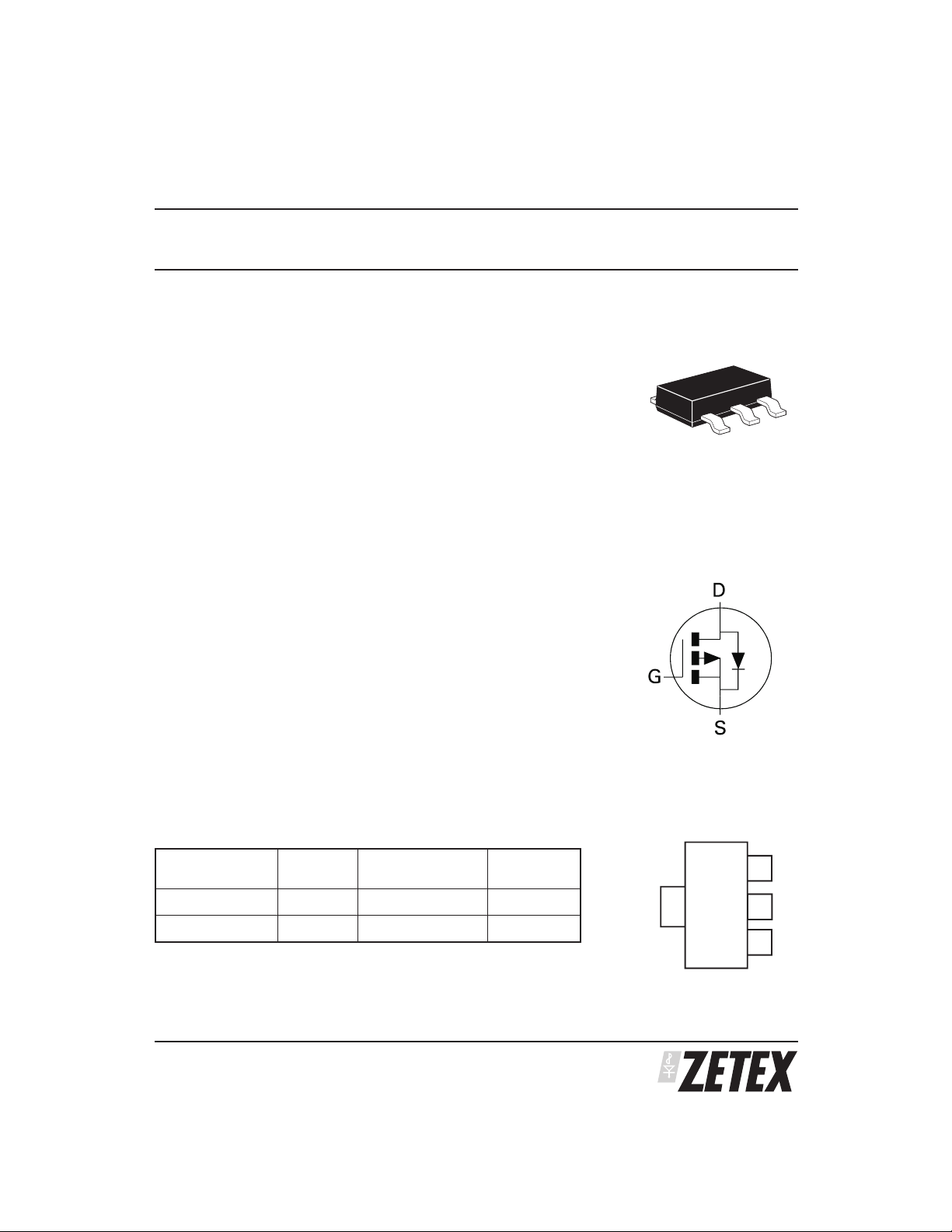
1
D
TOP VIEW
SEMICONDUCTORS
S
D
G
Page 2
ZVP4525G
ABSOLUTE MAXIMUM RATINGS.
PARAMETER SYMBOL LIMIT UNIT
V
(a)
(a)
I
I
I
P
DSS
GS
D
D
DM
S
SM
D
Drain-source voltage
Gate source voltage V
Continuous drain current (V
=10V; TA=25°C)
GS
(VGS=10V; TA=70°C)
Pulsed drain current
(c)
Continuous source current (body diode) I
Pulsed source current (body diode) I
(a)
Power dissipation at T
=25°C
A
Linear derating factor
Operating and storage temperature range T
j:Tstg
THERMAL RESISTANCE
PARAMETER SYMBOL VALUE UNIT
Junction to ambient
Junction to ambient
NOTES:
(a) For a device surface mounted on 25mm x 25mm FR4 PCB with high coverage of single sided 1oz copper, in still air conditions
(b) For a device surface mounted on FR4 PCB measured at t⭐5 secs.
(c) Repetitive rating - pulse width limited by maximum junction temperature. Refer to Transient Thermal Impedance graph.
(a)
(b)
R
θJA
R
θJA
250 V
±40
-265
-212
mA
mA
-1 A
-0.75 A
-1 A
2
16
mW/°C
-55 to +150 °C
63 °C/W
26 °C/W
V
W
NB High voltage applications
For high voltage applications, the appropriate industry sector guidelines should be considered with regard to
voltage spacing between conductors.
ISSUE 4 - JUNE 2004
SEMICONDUCTORS
2
Page 3
CHARACTERISTICS
ZVP4525G
ISSUE 4 - JUNE 2004
3
SEMICONDUCTORS
Page 4

ZVP4525G
ELECTRICAL CHARACTERISTICS (atT
= 25°C unless otherwise stated)
amb
PARAMETER SYMBOL MIN. TYP. MAX. UNIT CONDITIONS
STATIC
Drain-source breakdown voltage V
Zero gate voltage drain current I
Gate-body leakage I
Gate-source threshold voltage V
Static drain-source on-state resistance
Forward transconductance
DYNAMIC
(3)
(3)
(1)
Input capacitance C
Output capacitance C
Reverse transfer capacitance C
SWITCHING
(2) (3)
Turn-on delay time t
Rise time t
Turn-off delay time t
Fall time t
Total gate charge Q
Gate-source charge Q
Gate drain charge Q
(BR)DSS
DSS
GSS
GS(th)
R
DS(on)
g
fs
iss
oss
rss
d(on)
r
d(off)
f
g
gs
gd
-250 -285 V ID=-1mA, VGS=0V
-30 -500 nA VDS=-250V, VGS=0V
±1 ±100 nA
V
=±40V, VDS=0V
GS
-0.8 -1.5 -2.0 V ID=-1mA, VDS=V
10
13
14
18
V
Ω
Ω
=-10V, ID=-200mA
GS
V
=-3.5V,
GS
I
=-100mA
D
80 200 mS VDS=-10V,ID=-0.15A
73 pF
V
=-25 V, VGS=0V,
12.8 pF
DS
f=1MHz
3.91 pF
1.53 ns
V
=-30V, ID=-200mA
3.78 ns
17.5 ns
DD
R
=50Ω,VGS=-10V
G
(refer to test circuit)
7.85 ns
2.45 3.45 nC
V
=-25V,VGS=-10V,
0.22 0.31 nC
0.45 0.63 nC
DS
I
=-200mA(refer to
D
test circuit)
SOURCE-DRAIN DIODE
Diode forward voltage
Reverse recovery time
Reverse recovery charge
NOTES:
(1) Measured under pulsed conditions. Width=300µs. Duty cycle ≤ 2%.
(2) Switching characteristics are independent of operating junction temperature.
(3) For design aid only, not subject to production testing.
(1)
(3)
(3)
V
SD
t
rr
Q
rr
205 290 ns Tj=25°C, IF=-200mA,
21 29 nC
0.97 V Tj=25°C, IS=-200mA,
V
=0V
GS
di/dt= 100A/µ s
GS
SEMICONDUCTORS
ISSUE 4 - JUNE 2004
4
Page 5

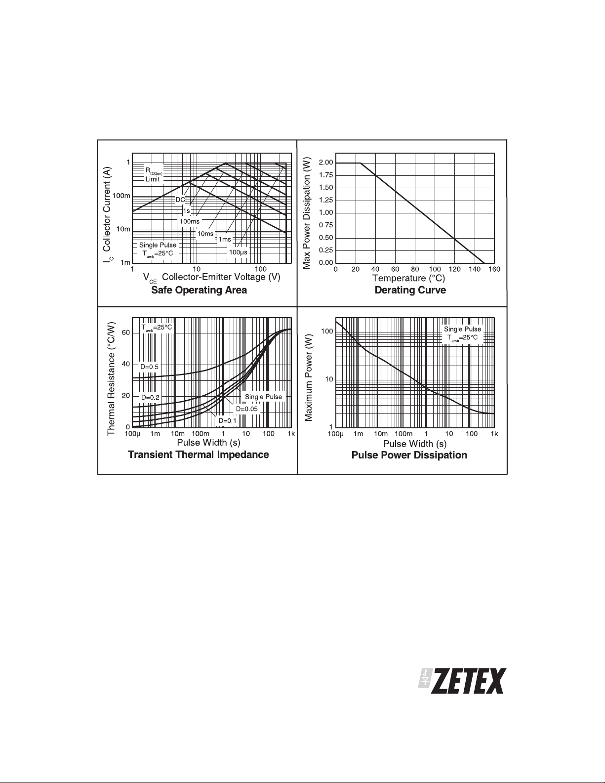
TYPICAL CHARACTERISTICS
ZVP4525G
ISSUE 4 - JUNE 2004
5
SEMICONDUCTORS
Page 6

ZVP4525G
CHARACTERISTICS
SEMICONDUCTORS
ISSUE 4 - JUNE 2004
6
Page 7

TEST CIRCUITS
Current
Regulator
ZVP4525G
V
GS
10%
90%
V
DS
Q
G
10V
Q
GS
V
G
Q
GD
Charge
BasicGateChargeWaveform
t
d(on)
t
r
Switching Time Waveforms
t
d(off)
12V 0.2µF
50k
I
Same as
D.U.T
0.3µF
V
G
D.U.T
V
GS
DS
I
D
Gate Charge Test Circuit
R
D
V
GS
R
G
-10V
t
f
Pulse Width < 1µS
≤
Duty Factor 0.1%
V
DS
V
cc
Switching Time Test Circuit
ISSUE 4 - JUNE 2004
7
SEMICONDUCTORS
Page 8

ZVP4525G
PACKAGE OUTLINE
PAD LAYOUT DETAILS
Controlling dimensions are in millimeters. Approximate conversions are given in inches
PACKAGE DIMENSIONS
DIM
Millimeters Inches
Min Max Min Max Min Max Min Max
DIM
A - 1.80 - 0.071 e 2.30 BSC 0.0905 BSC
A1 0.02 0.10 0.0008 0.004 e1 4.60 BSC 0.181 BSC
b 0.66 0.84 0.026 0.033 E 6.70 7.30 0.264 0.287
b2 2.90 3.10 0.114 0.122 E1 3.30 3.70 0.130 0.146
C 0.23 0.33 0.009 0.013 L 0.90 - 0.355 D 6.30 6.70 0.248 0.264 - ----
Millimeters Inches
© Zetex Semiconductors plc 2004
Europe
Zetex GmbH
Streitfeldstraße 19
D-81673 München
Germany
Telefon: (49) 89 45 49 49 0
Fax: (49) 89 45 49 49 49
europe.sales@zetex.com
These offices are supported by agents and distributors in major countries world-wide.
Thispublication isissued toprovideoutline informationonlywhich (unlessagreed bytheCompany inwriting)may notbe used,appliedor reproduced
for any purpose or form part of any order or contract or be regarded as a representation relating to the products or services concerned. The Company
reserves the right to alter without notice the specification, design, price or conditions of supply of any product or service.
For the latest product information, log on to www.zetex.com
Americas
Zetex Inc
700 Veterans Memorial Hwy
Hauppauge, NY 11788
USA
Telephone: (1) 631 360 2222
Fax: (1) 631 360 8222
usa.sales@zetex.com
Asia Pacific
Zetex (Asia) Ltd
3701-04 Metroplaza Tower 1
Hing Fong Road, Kwai Fong
Hong Kong
Telephone: (852) 26100 611
Fax: (852) 24250 494
asia.sales@zetex.com
Corporate Headquarters
Zetex plc
Lansdowne Road, Chadderton
Oldham, OL9 9TY
United Kingdom
Telephone (44) 161 622 4444
Fax: (44) 161 622 4446
hq@zetex.com
ISSUE 4 - JUNE 2004
SEMICONDUCTORS
8
 Loading...