

Page 1
P-CHANNEL ENHANCEMENT
Switc
easured
50Ω source
pedance and <5ns
ato
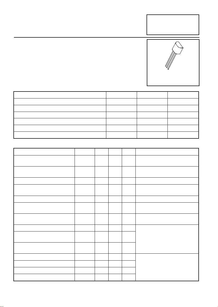
ZVP3310A
MODE VERTICAL DMOS FET
ISSUE 2 MARCH 94
FEATURES
* 100 Volt V
*R
DS(on)
ABSOLUTE MAXIMUM RATINGS.
PARAMETER SYMBOL VALUE UNIT
Drain-Source Voltage V
Continuous Drain Current at T
Pulsed Drain Current I
Gate Source Voltage V
Power Dissipation at T
Operating and Storage Temperature Range T
=20Ω
DS
=25°C I
amb
=25°C P
amb
DS
D
DM
GS
tot
j:Tstg
D
G
S
E-Line
TO92 Compatible
-100 V
-140 mA
-1.2 A
± 20
625 mW
-55 to +150 °C
V
ELECTRICAL CHARACTERISTICS (at T
= 25°C unless otherwise stated).
amb
PARAMETER SYMBOL MIN. MAX. UNIT CONDITIONS.
Drain-Source Breakdown
BV
Voltage
Gate-Source Threshold
Voltage
Gate-Body Leakage I
Zero Gate Voltage Drain
Current
On-State Drain Current(1) I
Static Drain-Source On-State
Resistance (1)
Forward Transconductance
(1)(2)
Input Capacitance (2) C
Common Source Output
Capacitance (2)
Reverse Transfer
Capacitance (2)
Turn-On Delay Time (2)(3) t
Rise Time (2)(3) t
Turn-Off Delay Time (2)(3) t
Fall Time (2)(3) t
V
GS(th)
GSS
I
DSS
D(on)
R
DS(on)
g
fs
iss
C
oss
C
rss
d(on)
r
d(off)
f
(1) Measured under pulsed conditions. Width=300
(2) Sample test.
-100 V ID=-1mA, VGS=0V
DSS
-1.5 -3.5 V ID=-1mA, VDS= V
20 nA
-1
µA
-50
µA
=± 20V, V
V
GS
V
=-100V, VGS=0
DS
V
=-80V, VGS=0V, T=125°C(2)
DS
-300 mA VDS=-25 V, VGS=-10V
20
VGS=-10V,ID=-150mA
Ω
50 mS VDS=-25V,ID=-150mA
50 pF
15 pF VDS=-25V, VGS=0V, f=1MHz
5pF
8ns
8ns
8ns
V
DD
8ns
µs. Duty cycle ≤2%
≈-25V, I
3-432
hing times m
with
im
rise time on a pulse gener
GS
=0V
DS
=-150mA
D
(
3
)
r
Page 2
S
tcgt
es
easu
edt50
sou
ce
pedacead5sseteoapusegee
ato
ZVP3310A
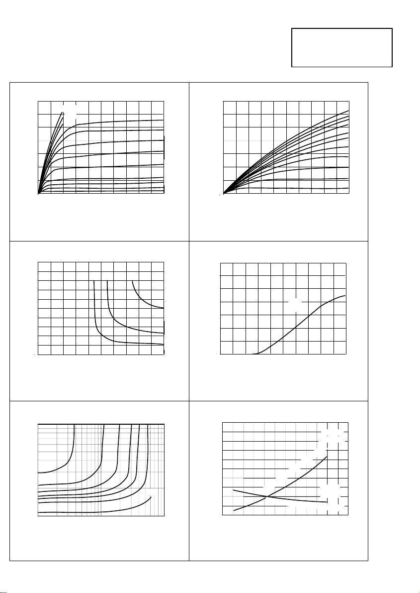
TYPICAL CHARACTERISTICS
VGS=-20V
-0.6
Amps)
(
nt
-0.4
e
r
r
u
in C
-0.2
a
r
D
-
D
I
0
-10
-8
-6
Voltage (Volts)
-4
-2
Drain Source
0
DS-
V
-16V
-12V
0 -10 -20 -30 -40 -50
VDS - Drain Source Voltage (Volts)
Output Characteristics
0-2-4-6-8-10
VGS-Gate Source Voltage (Volts)
Vo ltag e Sa turation Characteristics
-10V
-9V
-8V
-7V
-6V
-5V
-4.5V
-4V
-3.5V
ID=
-0.3A
-0.15A
-0.075A
ZVP3310A
-0.6
-0.4
-0.2
- Drain Current (Amps)
D
I
Amps)
(
nt
e
r
r
u
in C
a
r
D
-
D
I
0
-0.6
-0.4
-0.2
0
-2 -4 -6 -8 -10
VDS - Drain Source Voltage (Volts)
Saturation Characteristics
VDS=
-10V
0-2 -4 -6 -8 -10
V
GS-Gate Source Voltage (Volts)
Transfer Characteristics
VGS=
-20V
-16V
-14V
-12V
-10V
-9V
-8V
-7V
-6V
-5V
-4V
(Ω)
10
RDS(on)-Drain Source On Resistance
VGS=-4V
100
50
-10
ID-Drain Current (mA)
On-resistance v drain current
-8V
-7V
-10V
-20V
-6V
-5V
-100 -1000
2.6
2.4
2.2
GS(th)
2.0
and V
1.8
DS(on)
d R
e
malis
r
No
1.6
1.4
1.2
1.0
0.8
0.6
-40
-20 0 20 40 60 80
e R
rc
u
o
S
-
ain
Dr
Ga
t
e
T
h
r
e
Tj-Junction Temperature (°C)
Normalised R
DS(on)
and V
3-433
R
tance
s
i
s
e
s
h
o
ld
V
o
l
t
120
100 140 160
GS(th)
v Temperature
VGS=-10V
ID=-150mA
)
n
S(o
D
VGS=VDS
ID=-1mA
ag
e
V
GS
(
T
H
)
180
Page 3

TYPICAL CHARACTERISTICS
ZVP3310A
100
100
90
90
S)
m
80
80
(
e
70
70
c
n
60
60
50
50
ducta
40
40
n
o
c
30
30
20
20
ans
r
10
10
-T
s
f
0
0
g
0 -0.1 -0.2 -0.3 -0.4 -0.5 -0.6 -0.7 -0.8
0 -0.1 -0.2 -0.3 -0.4 -0.5 -0.6 -0.7 -0.8
ID- Drain Current (Amps)
Transconductance v drain current
50
40
)
F
p
(
30
e
c
n
ita
20
10
C-Capac
0
0 -10 -20 -30 -40 -50 -60 -70 -80
VDS-Drain Source Voltage (Volts)
Capacitance v drain-source voltage
V
DS=
V
DS=
V
GS=
f
=1MHz
-10V
-10V
0V
100
90
80
70
nce (mS)
60
50
ucta
40
nd
o
30
sc
20
an
r
T
10
-
fs
g
0
0-1-2-3-4-5-6-7-8-9-10
V
DS=
-10V
VGS-Gate Source Voltage (Volts)
Transconductance v gate-source voltage
0
-2
olts)
V
(
ge
olta
ce V
C
iss
C
oss
C
rss
r
Sou
e
Gat
-
GS
V
VDS=
-4
-25V
-6
-8
-10
-12
-14
-16
0.1 0.2 0.3 0.4 0.5 0.6
0
-50V
-100V
0.7 0.8 0.9 1.0 1.1 1.2
I
D=-
0.2A
Q-Charge (nC)
Gate charge v gate-source voltage
3-434
 Loading...