

Page 1
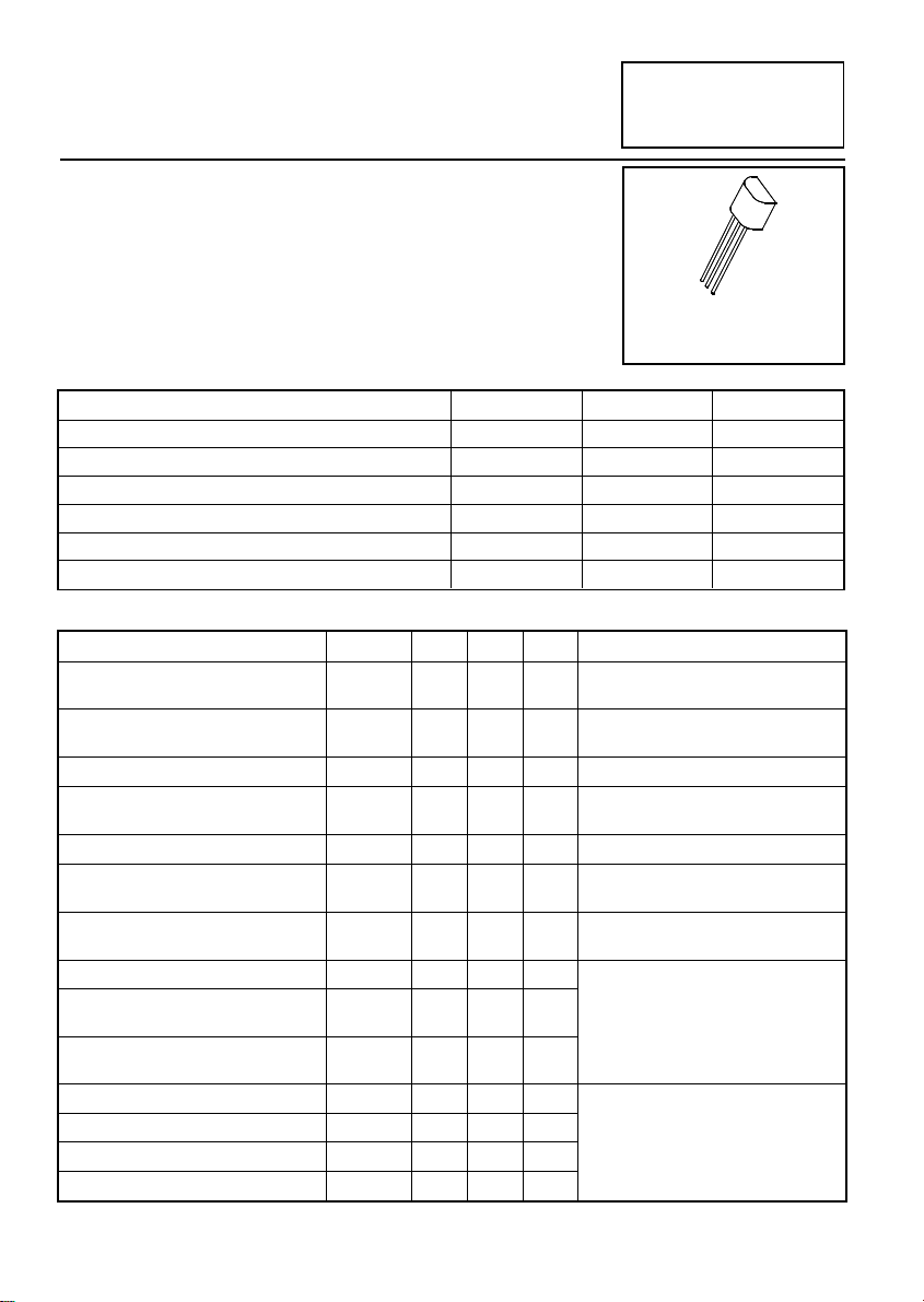
N-CHANNEL ENHANCEMENT
D
G
S
MODE VERTICAL DMOS FET
ISSUE 2 – MARCH 94
FEATURES
* 200 Volt V
*R
DS(on)
* Low threshold
APPLICATIONS
* Telephone handsets
ABSOLUTE MAXIMUM RATINGS.
PA RAM ETE R SY MBO L VALUE UNIT
Drain-Source Voltage V
Continuous Drain Current at T
Pulsed Drain Current I
Gate Source Voltage V
Power Dissipation at T
Operating and Storage Temperature Range T
=10Ω
DS
=25°C I
amb
=25°C P
amb
DS
D
DM
GS
tot
j:Tstg
ZVNL120A
E-Line
TO92 Compatible
200 V
180 mA
2A
± 20
700 mW
-55 to +150 °C
V
ELECTRICAL CHARACTER ISTI CS (at T
= 25°C unless otherwise stated).
amb
PARAMETER SYMBOL MIN. MAX. UNIT CONDITIONS.
Drain-Source Breakdown
Voltage
Gate-Source Threshold
Voltage
Gate-Body Leakage I
Zero Gate Voltage D rain
Current
On-State Drain Current(1) I
Static Drain-Source On-State
Resistance (1)
Forward Transconductance
(1)(2)
Input Capacitance (2) C
Common Source Output
Capacitance (2)
Reverse Transfer Capacitance
(2)
Turn-On Delay Time (2)(3) t
Rise Time (2)(3) t
Turn-Off Delay Time (2)(3) t
Fall Time (2)(3) t
BV
V
GS(th)
GSS
I
DSS
D(on)
R
DS(on)
g
fs
iss
C
oss
C
rss
d(on)
r
d(off)
f
200 V ID=1mA, VGS=0V
DSS
0.5 1.5 V ID=1mA, VDS= V
100 nA
10
100
V
GS
VDS=200 V, VGS=0
µA
V
µA
DS
500 mA VDS=25 V, VGS=5V
10
10
VGS=5V,ID=250mA
Ω
V
Ω
GS
200 mS VDS=25V,ID=250mA
85 pF
20 pF VDS=25 V, VGS=0V, f=1MHz
7pF
8ns
8ns
20 ns
V
DD
12 ns
GS
=± 20V, VDS=0V
=160 V, VGS=0V, T=125°C(2)
=3V, ID=125mA
≈25V, ID=250mA
(1) Measured under pulsed conditions. Width=300µs. Duty cycle ≤2% (2) Sample test.
(3) Switching times measured with 50Ω source impedance and <5ns rise time on a pulse generator
3-401
Page 2
D
G
S
ZVNL120A
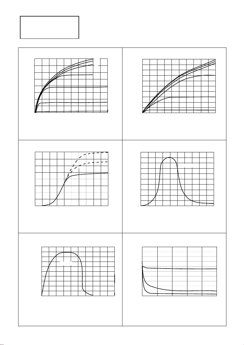
TYPICAL CHARACTERISTICS
1.6
)
s
1.4
1.2
t (Amp
en
1.0
r
r
u
0.8
C
n
i
a
0.6
Dr
)
0.4
n
O
D(
0.2
I
0
0 5 10 15 20 25 30 35 40 45 50
VDS - Drain Source Voltage (Volts)
Output Characteristics
1.6
)
1.4
1.2
Amps
1.0
nt (
e
r
r
0.8
u
C
n
0.6
i
a
Dr
0.4
)
n
O
0.2
D(
I
0
012345678910
GS-
V
Gate Source
Voltage (Volts)
Transfer Characteristics
VGS=
10V
8V
6V
5V
3V
2V
4V
VDS=
40V
20V
10V
1.0
0.8
0.6
0.4
Drain Current (Amps)
)
0.2
n
O
D(
I
0
0246810
VDS - Drain Source Voltage (Volts)
Saturation Characteristics
500
400
300
200
100
ransconductance (mS)
-T
fs
g
0
12345678910
VDS=25V
VGS-Gate Source Voltage (Volts)
Transconductance v gate-source voltage
VGS=
10V
8V
6V
4V
3V
2V
500
)
400
mS
(
e
c
n
ducta
n
o
sc
an
r
T
-
fs
g
300
200
100
0
VDS=25V
0.4
0.2
0
0.6 0.8 1.0
1.2
ID- Drain Current (Amps)
Transconductance v drain current
1.4
1.6 1.8 2.0
3-402
100
)
80
F
p
(
e
60
c
n
ita
c
40
Capa
20
C-
0
10 20
30
VDS-Drain Source Voltage (Volts)
Capacitance v drain-source voltage
40 50
Ciss
Coss
Crss
Page 3

TYPICAL CHARACTERISTICS
ZVNL120A
)
Ω
16
14
olts)
12
10
-Gate Source Voltage (V
S
G
V
ID= 700mA
8
6
4
2
0
0.4 0.8 1.2 1.6 2.0 2.4
0
Q-Charge (nC)
VDS=
50V
100V
150V
100
10
-Drain Source On Resistance (
1
DS(on)
R
Gate charge v gate-source voltage
)
Ω
100
(
10
ID=
1A
0.5A
0.1A
-Drain Source Resistance
1
DS(ON)
11020
R
VGS-Gate Source Voltage (Volts)
On-resistance vs gate-source voltage
2.4
2.2
h)
S(t
2.0
G
1.8
1.6
and V
1.4
DS(on)
1.2
R
1.0
d
0.8
ise
0.6
mal
r
0.4
No
Normalised R
VGS=2V
10
ID-Drain Current
3V
100
(mA)
On-resistance v drain current
VGS=5V
-60
-80
-40
ID=250mA
o
S
-
n
Drai
Gate
T
h
-20 0 20 40 60 80
Tj-Junction Temperature (C°)
DS(on)
and V
e
c
n
ta
s
i
s
e
R
e
c
r
u
res
h
o
l
d
V
o
l
tag
100 140 160
GS(th)
vs Temperature
n
o
DS(
R
VGS=3V
ID=125mA
VGS=VDS
ID=1mA
e
V
120
4V
5V
10V
1000
)
GS
(
th
)
3-403
 Loading...