

Page 1
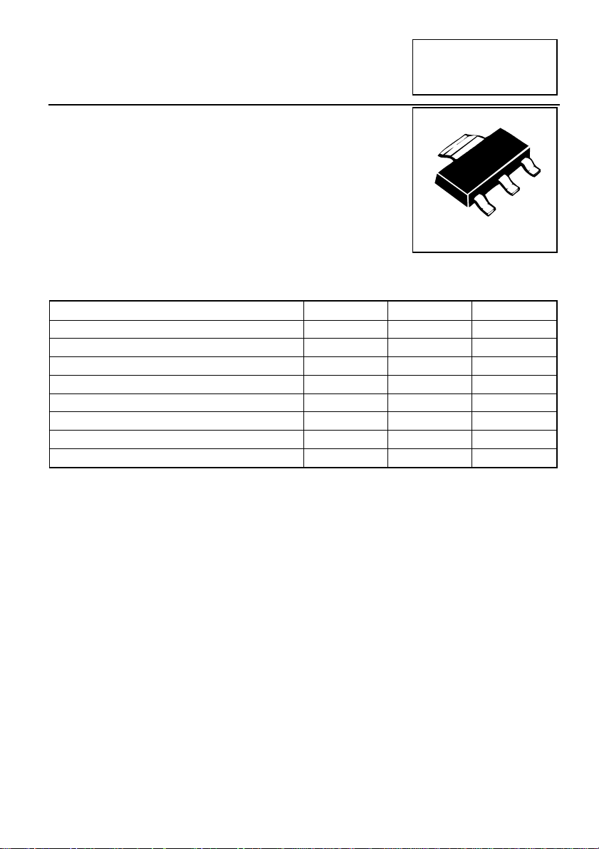
SOT223 N-CHANNEL ENHANCEMENT
G
MODE VERTICAL DMOS FET
ISSUE 1 - APRIL 1998
FEATURES
*BV
*R
* Repetitive Avalanche Rating
APPLICATIONS
* DC - DC Converters
* Solenoids/Relay Drivers for Automotive
* Stepper Motor Drivers
PARTMARKING DETAIL - ZVN4306V
ABSOLUTE MAXIMUM RATINGS.
PARAMETER SYMBOL VALUE UNIT
Drain-Source Voltage V
Continuous Drain Current at T
Pulsed Drain Current I
Gate Source Voltage V
Power Dissipation at T
Avalanche Current-Repetitive I
Avalanche Energy-Repetitive E
Operating and Storage Temperature Range T
DSS
DS(ON)
=60V
= 0.33Ω
=25°C I
amb
=25°C P
amb
DS
D
DM
GS
tot
AR
AR
j:Tstg
ZVN4306GV
D
60 V
2.1 A
15 A
± 20
3W
1A
25 mJ
-55 to +150 °C
S
D
V
Page 2
ZVN4306GV
ELECTRICAL CHARACTERISTICS (at T
= 25°C unless otherwise stated).
amb
PARAMETER SYMBOL MIN. TYP. MAX. UNIT CONDITIONS.
Drain-Source
Breakdown Voltage
Gate-Source
Threshold Voltage
Gate-Body Leakage I
Zero Gate Voltage
Drain Current
On-State Drain
Current(1)
Static Drain-Source
On-State Resistance
(1)
Forward
Transconductance (1)
Input Capacitance (2) C
Common Source
Output Capacitance
BV
V
GS(th)
GSS
I
DSS
I
D(on)
R
DS(on)
g
fs
iss
C
oss
60 V ID=1mA, VGS=0V
DSS
1.3 3 V ID=1mA, VDS= V
20 nA
10
100
V
VDS=60V, VGS=0V
µA
V
µA
12 A VDS=10V, VGS=10V
0.22
0.32
0.33
0.45
VGS=10V, ID=3A
Ω
V
Ω
0.7 S VDS=25V,ID=3A
350 pF
140pFVDS=25 V, VGS=0V, f=1MHz
GS
=± 20V, VDS=0V
GS
=48V, VGS=0V, T=125°C(2)
DS
=5V, ID=1.5A
GS
(2)
Reverse Transfer
Capacitance (2)
Turn-On Delay Time
(2)(3)
Rise Time (2)(3) t
Turn-Off Delay Time
(2)(3)
Fall Time (2)(3) t
C
rss
t
d(on)
r
t
d(off)
f
30 pF
8ns
25 ns
V
30 ns
16 ns
≈25V, V
DD
=10V, ID=3A
GEN
(1) Measured under pulsed conditions. Width=300µs. Duty cycle ≤2% (2) Sample test.
(3) Switching times measured with 50Ω source impedance and <5ns rise time on a pulse generator
Spice parameter data is available upon request for this device
Page 3

TYPICAL CHARACTERISTICS
GS=
V
10V
12V
20V
012345678910
DS
V
- Drain Source
s)
(Amp
t
ren
n Cur
i
a
- Dr
D
I
12
11
10
9
8
7
6
5
4
3
2
1
0
Saturation Characteristics
2.6
h)
t
2.4
GS(
2.2
V
2.0
nd
a
1.8
)
n
1.6
S(o
D
R
1.4
1.2
sed
i
1.0
al
m
0.8
or
N
0.6
Gate Threshold Voltage VGS(TH)
-50
-25 0 25 50 75
Normalised R
9V
8V
Voltage (Volts)
ce
an
st
si
urce Re
o
S
Drain-
100
125 175 200
Tj-Junction Temperature (°C)
DS(on)
and V
GS(th)
VGS=10V
ID=3A
on)
S(
D
R
VGS=VDS
ID=1mA
150
v Temp erature
7V
6V
5V
4V
3.5V
3V
225
ZVN4306GV
ID-Drain Current
2
4
0
D(on)
I
3.5V
5V
1
(Amps)
DS=
V
10V
6810
- Drain Current (Amps
VGS=3V 6V
10
(Ω)
1.0
0.1
0.1
RDS(on)-Drain Source On Resistan ce
On-resistance v drain current
5
)
4
S
(
3
nce
ucta
2
nd
sco
1
-Tran
s
f
0
g
Transconductance v drain current
8V
10V
10
121416 18 20
100
)
500
400
)
300
ce (pF
tan
200
ci
a
100
C-Cap
0
01020304050607080
VDS-Drain Source Voltage (Volts)
Capacitance v drain-source voltage
C
Coss
Crss
16
14
ts)
ol
V
(
ge
ta
iss
ol
ce V
r
ou
-Gate S
GS
V
ID=3A
12
10
8
6
4
2
0
123456789101112
0
VDD=
20V
40V
60V
Q-Charge (nC)
Gate charge v gate-source voltage
Page 4

ZVN4306GV
 Loading...