

Page 1
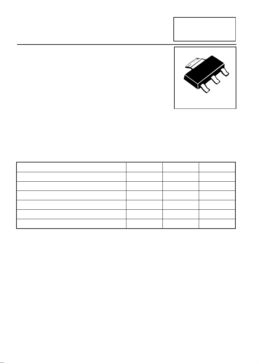
SOT223 N-CHANNEL ENHANCEMENT
MODE VERTICAL DMOS FET
ISSUE 3 - JANUARY 1996 ✪
FEATURES
* Compact geometry
* Fast switching speeds
* No secondary breakdown and Excel lent temper atur e stabi lity
* High input impedance and low current drive
* Ease of parralleling
APPLICATIONS
* DC-DC converters
* Solenoid / relay drivers for automotive applicat ions
* Stepper motor drivers and Print he ad drivers
PARTMARKING DETAIL - ZVN4206
ABSOLUTE MAXIMUM RATINGS.
PARAMETER SYMBOL VALUE UNIT
Drain-Source Voltage V
Continuous Drain Current at T
Pulsed Drain Current I
Gate-Source Voltage V
Power Dissipation at T
Operating and Storage Temperature Range T
amb
=25°C I
amb
=25°C P
DS
D
DM
GS
tot
j:Tstg
ZVN4206G
D
G
60 V
1A
8A
± 20
2W
-55 to +150 °C
S
D
V
Page 2
ZVN4206G
ELECTRICAL CHARACTERISTICS (at T
= 25°C unless otherwise stated).
amb
PARAMETER SYMBOL MIN. MAX. UNIT CONDITIONS.
Drain-Source Breakdown Voltage BV
Gate-Source Threshold Voltage V
Gate-Body Leakage I
Zero Gate Voltage Drain Current I
On-State Drain Current (1) I
Static Drain-Source On-State
Resistance (1)
Forward Transconductance (1)(2) g
Input Capacitance (2) C
Common Source Output
Capacitance (2)
Reverse Transfer Capacitance (2) C
Turn-On Delay Time (2)(3) t
Rise Time (2)(3) t
Turn-Off Delay Time (2)(3) t
Fall Time (2)(3) t
(1) Measured under pulsed conditions. Width=300µs. Duty cycle ≤2%
(2) Sample test.
GSS
DSS
D(on)
R
C
d(on)
r
d(off)
f
GS(th)
DS(on)
fs
iss
oss
rss
60 V ID=1mA, VGS=0V
DSS
1.3 3 V ID=1mA, VDS= V
100 nA
10
µA
100
µA
3AV
1
Ω
1.5
Ω
300 mS VDS=25V,ID=1.5A
100 pF
60 pF VDS=25V, VGS=0V, f=1MHz
20 pF
8ns
12 ns
12 ns
15 ns
GS
V
=± 20V, VDS=0V
GS
VDS=60V, VGS=0V
V
=48V, VGS=0V, T=125°C(2)
DS
=25V, VGS=10V
DS
VGS=10V, ID=1.5A
V
=5V, ID=0.5A
GS
V
≈25V, ID=1.5A, V
DD
GEN
=10V
(3) Switching times measured with 50Ω source im pedance and <5ns rise time on a pulse generator
3 - 402 3 - 401
Page 3

TYPICAL CHARACTERISTICS
ZVN4206G ZVN4206G
10
8
6
nt (Amps)
e
urr
4
C
n
i
a
r
2
D
-
D
I
0
V
GS=
20V
16V
14V
12V
010 20304050
V
DS
- Drain Source Voltage (Volts)
Output Characteristics
10
8
6
Voltage (Volts)
4
2
Drain Source
DS-
0
V
02 4 6 8 10
V
GS-
Gate Source Voltage (Volts)
Vo ltag e Saturation Characteris tics
10V
9V
8V
7V
6V
5V
4.5V
4V
3.5V
I
D=
3A
1.5A
0.5A
10
8
Amps)
6
t (
n
4
2
- Drain Curre
D
I
0
246810
V
DS
- Drain Source Voltage (Volts)
Saturation Characteristics
6
nt (Amps)
e
4
r
r
u
C
n
i
a
r
2
D
-
D
I
0
0246810
V
DS=
10V
V
GS-
Gate Source Voltage (Volts)
Transfer Characteristics
V
20V
16V
14V
12V
10V
9V
8V
7V
6V
5V
4.5V
3.5V
GS=
4V
1.0
0.1
GS
V
10
0.1
ID-Drain Current (Amps)
=3.5V
)
Ω
(
-Drain Source On Resistance
DS(on)
R
On-resistance v drain current
4.5V
8V
10V
6V
14V
20V
1.0
10
2.6
2.4
(th)
S
2.2
G
V
2.0
nd
a
1.8
n)
o
1.6
(
S
D
1.4
1.2
1.0
0.8
0.6
Normalised R
-50
u
o
-S
n
Drai
G
ate
T
h
res
-25 0 25 50 75
e R
rc
h
o
l
d
es
V
100 150
V
ID=1.5A
)
n
o
S(
D
e R
c
tan
s
i
o
lt
ag
e
V
GS
(
TH
125 175 200
GS=
V
GS=VDS
ID=1mA
)
10V
225
Tj-Junction Temperature (°C)
Normalised R
DS(on)
and V
GS(th)
v Temperature
3 - 403 3 - 404
Page 4

TYPICAL CHARACTERISTICS
1000
900
800
700
nce (mS)
600
a
t
c
500
400
ndu
o
300
sc
n
200
ra
100
T
-
fs
0
g
012345678910
V
DS=
10V
ID- Drain Current (Amps
Transconductance v drain current
200
160
120
nce (pF)
ita
c
80
a
Cap
40
C-
0
01020 304050607080
VDS-Drain Source Voltage (Volts)
Capacitance v drain-source voltage
1000
900
S)
800
m
700
ce (
n
600
500
ducta
400
n
o
300
c
200
rans
100
-T
s
f
0
g
012345678910
)
VGS-Gate Source Voltage (Volts)
V
DS=
10V
Transconduc ta n ce v ga te -source voltage
VDS=
60V
40V
16
olts)
oltage (V
V
C
iss
C
oss
C
rss
urce
So
te
a
-G
S
G
V
ID=1.5A
14
12
10
8
6
4
2
0
0.5 1.0 1.5 2.0 2.5 3.0 3.5 4.0 4.5 5.0 5.5 6.0
0
20V
Q-Charge (nC)
Gate charge v gate-source voltage
 Loading...