

Page 1
A
f
g
q
Please click here to visit our online spice models database.
Product Summary
V
(V)
DS
R
(Ω)
DS(ON)
100
10
Description and Applications
This MOSFET utilises a structure that combines low input
capacitance with relatively low on-resistance and has an intrinsically
higher pulse current handling capability in linear mode than a
comparable trench technology structure. This MOSFET is suitable for
general purpose applications.
• General purpose 100V FET
• Power management
• Disconnect switches
• Telecoms
• Complementary Type – ZVP3310F
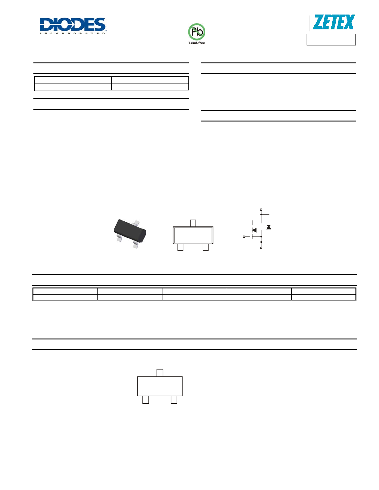
TOP VIEW
G
Pin Out Confi
SOT-23
D
TOP VIEW
Product Line o
Diodes Incorporated
ZVN3310F
100V N-CHANNEL ENHANCEMENT MODE MOSFET
Features and Benefits
• High pulse current handling in linear mode
• Low input capacitance
• Fast switching speed
• Lead Free By Design/RoHS Compliant (Note 1)
Mechanical Data
• Case: SOT-23
• Case Material: UL Flammability Classification Rating 94V-0
• Moisture sensitivity: Level 1 per J-STD-020
• Terminals: Matte Tin Finish annealed over Alloy 42 leadframe
(Lead Free Plating). Solderable per MIL-STD-202, Method 208
• Terminal Connections: See Diagram
• Weight: 0.008 grams (approximate)
Drain
Gate
S
uration
E
Source
uivalent Circuit
Ordering Information (Note 2)
Product Marking Reel size (inches) Tape width (mm) Quantity per reel
ZVN3310FTA MF 7 8 3000
Notes: 1. No purposefully added lead.
2. For packaging details, go to our website at http://www.diodes.com/datasheets/ap02007.pdf.
Marking Information
MF
MF = Product Type Marking Code
ZVN3310F
Document Number DS31980 Rev. 4 - 2
1 of 5
www.diodes.com
October 2009
© Diodes Incorporated
Page 2
A
f
)
)
)
)
r
)
Product Line o
Diodes Incorporated
ZVN3310F
Maximum Ratings @T
= 25°C unless otherwise specified
A
Characteristic Symbol Value Units
Drain-Source Voltage
Gate-Source Voltage
Continuous Drain Current
Pulsed Drain Current
V
DSS
V
GSS
I
D
I
DM
Thermal Characteristics
Characteristic Symbol Value Unit
Power Dissipation @TA = 25°C PD
Operating and Storage Temperature Range
Electrical Characteristics @T
= 25°C unless otherwise specified
A
Characteristic Symbol Min Typ Max Unit Test Condition
OFF CHARACTERISTICS
Drain-Source Breakdown Voltage
Zero Gate Voltage Drain Current TJ = 25°C
T
= 125°C (Note 4)
J
Gate-Source Leakage
Gate Threshold Voltage
BV
V
DSS
I
DSS
I
GSS
GS(th
100
⎯ ⎯
⎯ ⎯
0.8
ON CHARACTERISTICS (Note 3)
On-State Drain Current
Static Drain-Source On-Resistance
I
D (ON
R
DS (ON
500
⎯ ⎯
DYNAMIC CHARACTERISTICS (Note 4)
Forward Transconductance (Note 3) gfs 100
Input Capacitance
Output Capacitance
Reverse Transfer Capacitance
Turn-On Delay Time (Note 5)
Turn-On Rise Time (Note 5)
Turn-Off Delay Time (Note 5)
Turn-Off Fall Time (Note 5)
Notes: 3. Measured under pulsed conditions. Width = 300μs. Duty cycle ≤2%
4. Sample test.
5. Switching times measured with 50Ω source impedance and <5ns rise time on a pulse generator.
C
⎯ ⎯
iss
⎯ ⎯
⎯ ⎯
⎯
⎯
⎯
⎯
C
C
t
D(on
t
D(off
oss
rss
t
t
f
T
J, TSTG
⎯ ⎯
⎯
⎯ ⎯
⎯ ⎯
3 5
5 7
4 6
5 7
1
50
20 nA
2.4 V
10 Ω
40
15
5
100 V
±20 V
100 mA
2 A
330 mW
-55 to +150 °C
V
ID = 1mA, VGS = 0V
= 100V, VGS = 0V
V
μA
DS
V
= 80V, VGS = 0V
DS
VGS = ±20V, VDS = 0V
VDS = VGS, ID = 1mA
mA
VDS = 25V, VGS = 10V
VGS = 10V, ID = 500mA
mS
V
= 25V, ID = 500mA
DS
V
= 25V, VGS = 0V
pF
ns
DS
f = 1.0MHz
V
≈ 25V, ID = 500mA
DD
ZVN3310F
Document Number DS31980 Rev. 4 - 2
2 of 5
www.diodes.com
October 2009
© Diodes Incorporated
Page 3

A
f
Product Line o
Diodes Incorporated
ZVN3310F
ZVN3310F
Document Number DS31980 Rev. 4 - 2
3 of 5
www.diodes.com
October 2009
© Diodes Incorporated
Page 4

A
f
0.0
Package Outline Dimensions
Product Line o
Diodes Incorporated
ZVN3310F
E
e
Dim. Millimeters Inches Dim. Millimeters Inches
Min. Max. Min. Max. Min. Max. Min. Max.
A - 1.12 - 0.044 e1 1.90 NOM 0.075 NOM
A1 0.01 0.10 0.0004 0.004 E 2.10 2.64 0.083 0.104
b 0.30 0.50 0.012 0.020 E1 1.20 1.40 0.047 0.055
c 0.085 0.20 0.003 0.008 L 0.25 0.60 0.0098 0.0236
D 2.80 3.04 0.110 0.120 L1 0.45 0.62 0.018 0.024
e 0.95 NOM 0.037 NOM - - - - -
Note: Controlling dimensions are in millimeters. Approximate dimensions are provided in inches
Suggested Pad Layout
b
3leads
L1
A1
E1
e1
D
A
L
c
0.95
0.037
2.0
0.079
0.9
0.035
0.8
31
ZVN3310F
Document Number DS31980 Rev. 4 - 2
4 of 5
www.diodes.com
mm
inches
October 2009
© Diodes Incorporated
Page 5

A
f
Product Line o
IMPORTANT NOTICE
DIODES INCORPORATED MAKES NO WARRANTY OF ANY KIND, EXPRESS OR IMPLIED, WITH REGARDING TO THIS DOCUMENT,
INCLUDING, BUT NOT LIMITED TO, THE IMPLIED WARRANTIES OF MERCHANTABILITY AND FITNESS FOR A PARTICULAR PURPOSE
(AND THEIR EQUIVALENTS UNDER THE LAWS OF ANY JURISDICTION).
Diodes Incorporated and its subsidiaries reserve the right to make modifications, enhancements, improvements, corrections or other changes
without further notice to this document and any product described herein. Diodes Incorporated does not assume any liability arising out of the
application or use of this document or any product described herein; neither does Diodes Incorporated convey any license under its patent or
trademark rights, nor the rights of others. Any Customer or user of this document or products described herein in such applications shall assume
all risks of such use and will agree to hold Diodes Incorporated and all the companies whose products are represented on Diodes Incorporated
website, harmless against all damages.
Diodes Incorporated does not warrant or accept any liability whatsoever in respect of any products purchased through unauthorized sales channel.
Should Customers purchase or use Diodes Incorporated products for any unintended or unauthorize d application, Customers shall indemnify and
hold Diodes Incorporated and its representatives harmless against all claims, damages, expenses, and attorney fees arising out of, directly or
indirectly, any claim of personal injury or death associated with such unintended or unauthorized application.
Products described herein may be covered by one or more United States, international or foreign patents pending. Product names and markings
noted herein may also be covered by one or more United States, international or foreign trademarks.
LIFE SUPPORT
Diodes Incorporated products are specifically not authorized for use as critical components in life support devices or systems without the express
written approval of the Chief Executive Officer of Diodes Incorporated. As used herein:
A. Life support devices or systems are devices or systems which:
1. are intended to implant into the body, or
2. support or sustain life and whose failure to perform when properly used in accordance with instructions for use provided in the
labeling can be reasonably expected to result in significant injury to the user.
B. A critical component is any component in a life support device or system whose failure to perform can be reasonably expected to cause the
failure of the life support device or to affect its safety or effectiveness.
Customers represent that they have all necessary expertise in the safety and regulatory ramifications of their life support devices or systems, and
acknowledge and agree that they are solely responsible for all legal, regulatory and safety-related requirements concerning their products and any
use of Diodes Incorporated products in such safety-critical, life support devices or systems, notwithstanding any devices- or systems-related
information or support that may be provided by Diodes Incorporated. Further, Customers must fully indemnify Diodes Incorporated and its
representatives against any damages arising out of the use of Diodes Incorporated products in such safety-critical, life support devices or systems.
Copyright © 2009, Diodes Incorporated
www.diodes.com
Diodes Incorporated
ZVN3310F
ZVN3310F
Document Number DS31980 Rev. 4 - 2
5 of 5
www.diodes.com
October 2009
© Diodes Incorporated
 Loading...