Diodes ZTX796A User Manual

A
f
C
Product Line o
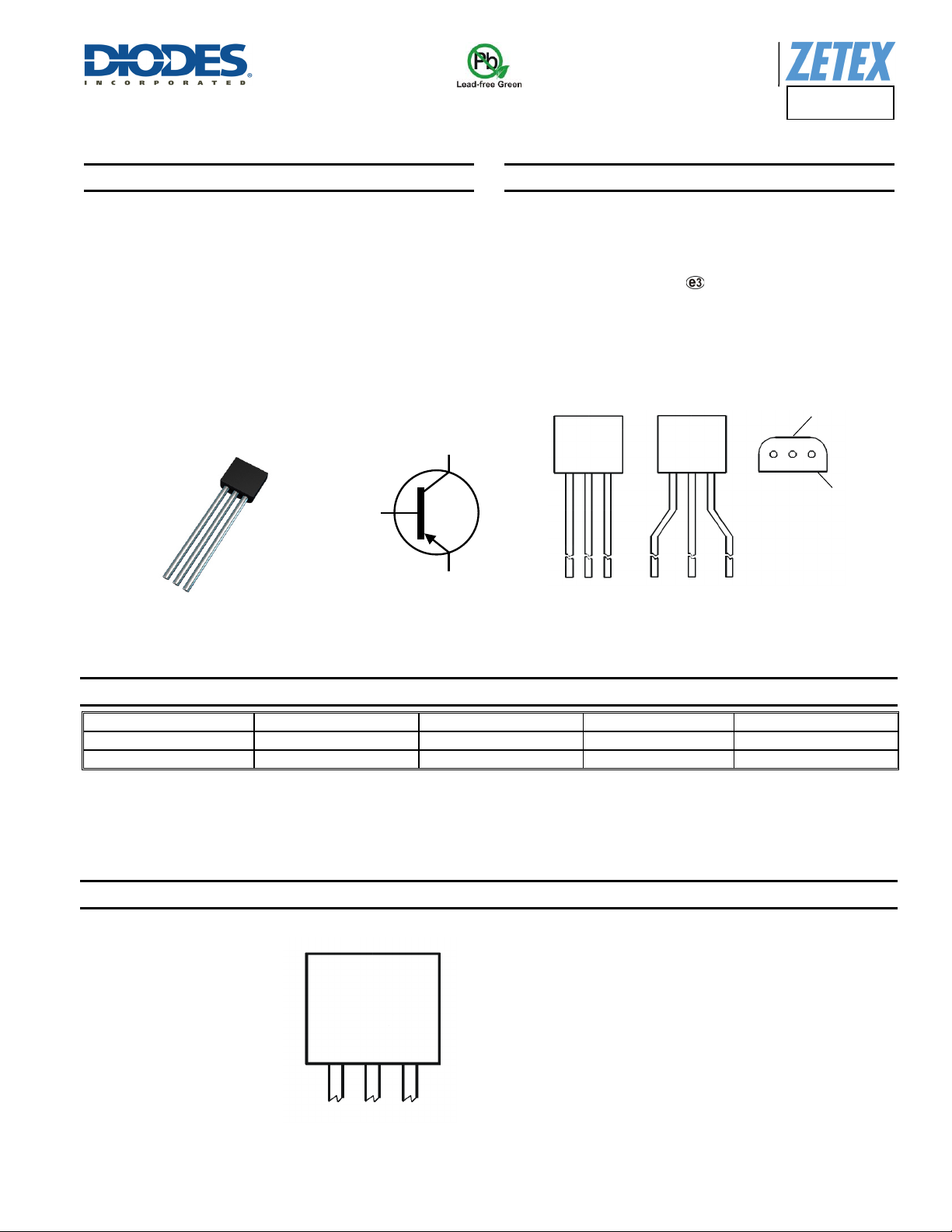
200V PNP MEDIUM POWER HIGH GAIN TRANSISTOR IN E-LINE
Features
Mechanical Data
Diodes Incorporated
ZTX796A
BV
I
I
T
h
P
Complementary NPN Type: ZTX696B
Totally Lead-Free & Fully RoHS compliant (Notes 1 & 2)
Halogen and Antimony Free. “Green” Device (Note 3)
Qualified to AEC-Q101 Standards for High Reliability
> -200V
CEO
= -0.5A High Continuous Collector Current
C
= -1A Peak Pulse Current
CM
up to 200°C for High Temperature Operation
J
> 250 @ 0.3A for High Gain Hold-Up
FE
= 1W Power dissipation
D
E-Line
(TO-92 Compatible)
Flat Face View
B
Device Symbol
Case: E-Line (TO-92 Compatible)
Case Material: molded plastic, “Green” Molding Compound
UL Flammability Classification Rating 94V-0
Terminals: Finish – Matte Tin Plated Leads, Solderable per
MIL-STD-202, Method 208
Weight: 0.159 grams (approximate)
Part Mark on
Rounded Face
E
Ejection Mark
on Flat Face
BC
Bottom View
E
BC
Rounded Face View
C
B
E
Pin-Out Configuration
E
Ordering Information (Note 4)
Product Marking Package Leads Quantity
ZTX796ASTZ ZTX796A E-Line Joggled 2,000 Taped per Ammo Box
ZTX796A ZTX796A E-Line Straight 4,000 Loose in a Box
Notes: 1. No purposely added lead. Fully EU Directive 2002/95/EC (RoHS) & 2011/65/EU (RoHS 2) compliant.
2. See http://www.diodes.com/quality/lead_free.html for more information about Diodes Incorporated’s definitions of Halogen- and Antimony-free, "Green"
and Lead-free.
3. Halogen- and Antimony-free "Green” products are defined as those which contain <900ppm bromine, <900ppm chlorine (<1500ppm total Br + Cl) and
<1000ppm antimony compounds.
4. For packaging details, go to our website at http://www.diodes.com/products/packages.html.
Marking Information
ZTX796A
Document Number DS31908 Rev. 3 - 2
ZTX
796A
Rounded Face View
ZTX796A = Product Type Marking Code
1 of 7
www.diodes.com
May 2013
© Diodes Incorporated

A
f
Maximum Ratings (@T
= +25°C, unless otherwise specified.)
A
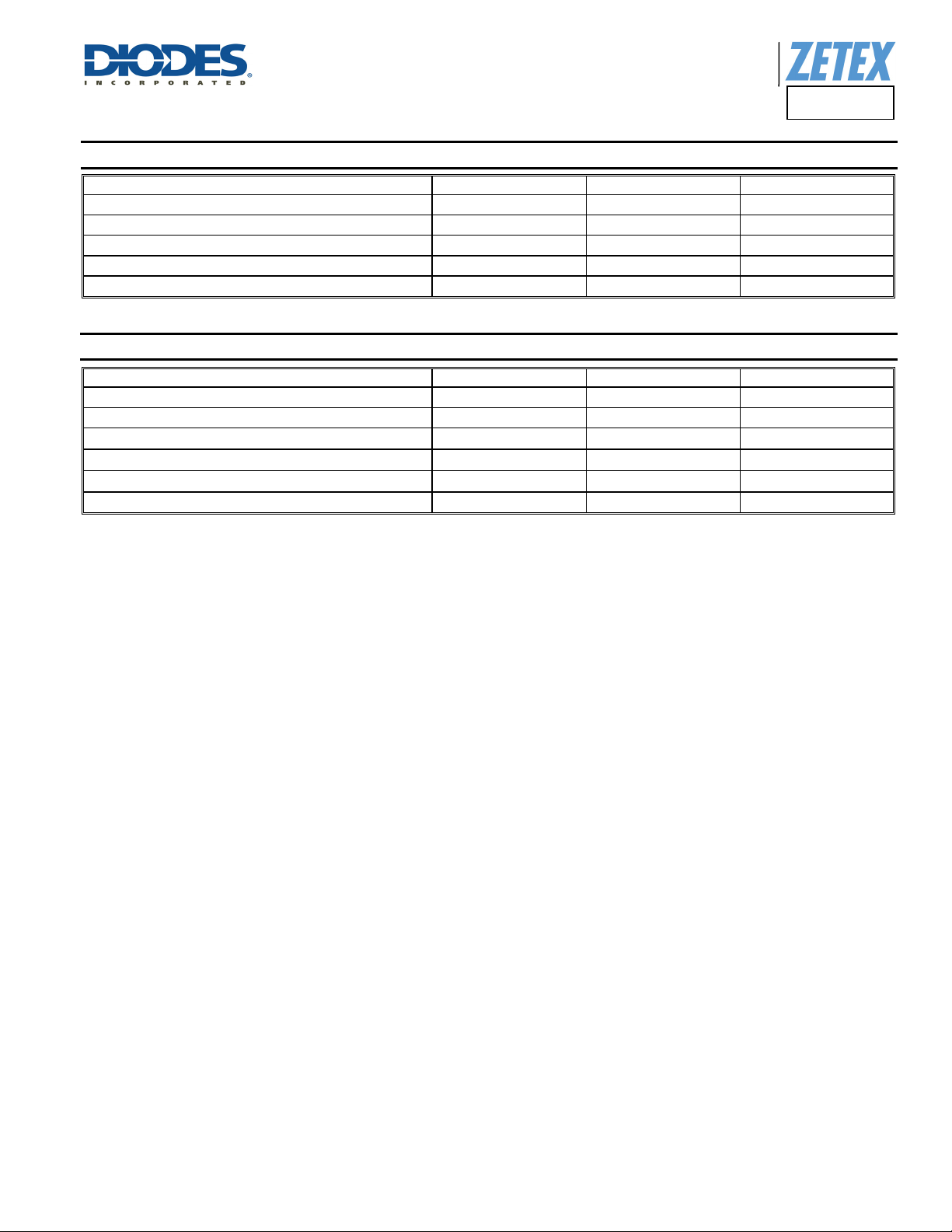
Characteristic Symbol Value Unit
Collector-Base Voltage
Collector-Emitter Voltage
Emitter-Base Voltage
Continuous Collector Current
Peak Pulse Current
V
CBO
V
CEO
V
EBO
I
C
I
CM
Thermal Characteristics (@T
= +25°C, unless otherwise specified.)
A
Characteristic Symbol Value Unit
Power Dissipation (Note 5)
Power Dissipation (Note 6)
Thermal Resistance Junction to Ambient (Note 5)
Thermal Resistance Junction to Ambient (Note 6)
Thermal Resistance Junction to Lead (Note 7)
Operating and Storage Temperature Range
Notes: 5. For a through-hole device mounted at the seating plane (2.5mm lead length) with the collector lead on 25mm x 25mm 1oz copper
that is on a single-sided FR4 PCB; device is measured under still air conditions whilst operating in a steady-state.
6. Same as note (5), except the device is mounted on minimum recommended pad layout with 12mm lead length from the bottom of package to the board.
7. Thermal resistance from junction to solder-point at the seating plane (2.5mm from the bottom of package along the collector lead).
P
P
R
R
R
T
J, TSTG
D
D
JA
JA
JL
Diodes Incorporated
-200 V
-200 V
-5 V
-0.5 A
-1 A
1.5 W
1 W
116 °C/W
175 °C/W
70 °C/W
-55 to +200 °C
Product Line o
ZTX796A
ZTX796A
Document Number DS31908 Rev. 3 - 2
2 of 7
www.diodes.com
May 2013
© Diodes Incorporated

A
f
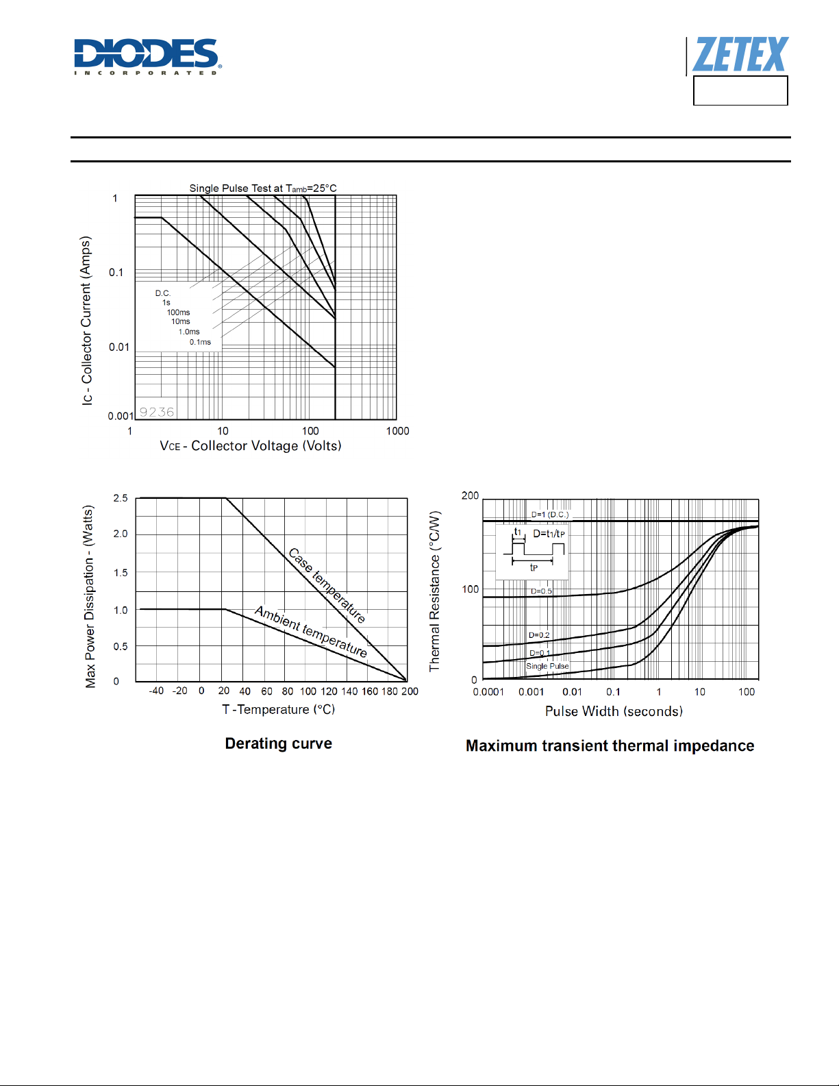
Thermal Characteristics and Derating Information
Product Line o
Diodes Incorporated
ZTX796A
ZTX796A
Document Number DS31908 Rev. 3 - 2
3 of 7
www.diodes.com
May 2013
© Diodes Incorporated
 Loading...