Diodes ZRT040 User Manual

4.01V LOW POWER PRECISION REFERENCE SOURCE
Description
The ZRT040 is a monolithic integrated circuit providing a
precise stable reference voltage of 4.01V at 500μA.
The circuit features a knee current of 150μA and operation
over a wide range of temperatures and currents.
The ZRT040 is available in a SOT223 package for surface
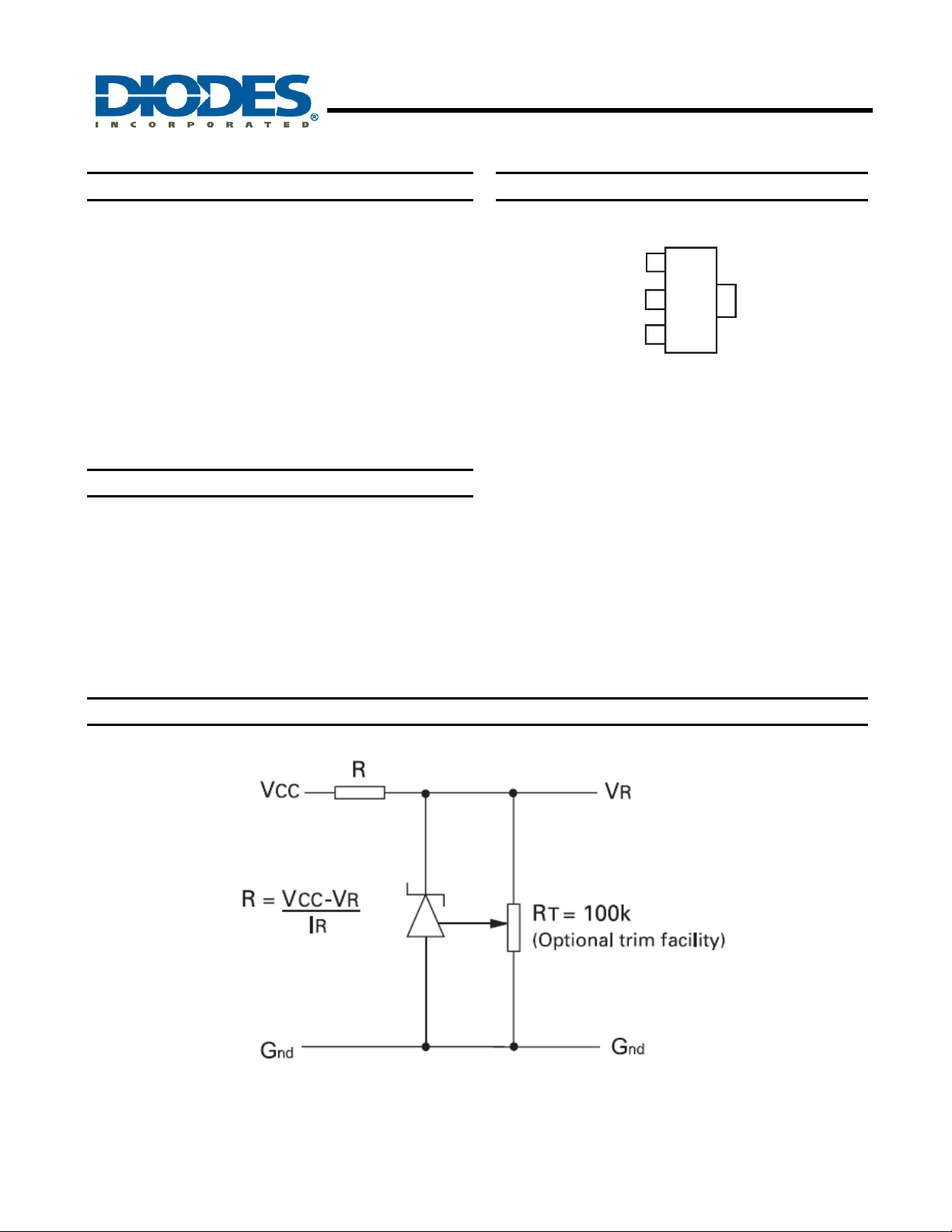
mount applications. This device offers a trim facility whereby
the output voltage can be adjusted as shown in the
schematic diagram. This facility is used when compensating
for system errors or setting the reference output to a
particular value. When the trim facility is not used, the pin
should be left open circuit.
Features
• Trimmable output
• Excellent temperature stability
• Low output noise figure
• -40 to 85°C operating temperature range
• 1% initial voltage tolerance
• No external stabilizing capacitor required in most cases
• Low slope resistance
• No derating required at low temperatures
• SOT223 package
Pin Assignments
T
RIM
GND
V
R
(Pin 4 floating or
connected to pin 2)
SOT223
1
2
3
Top View
ZRT040
4
Schematic Diagram
This circuit will allow the reference to be trimmed over a wide range. The device is specified over a ±5% trim range.
ZRT040
Document number: DS33258 Rev. 5 - 2
1 of 5
www.diodes.com
February 2011
© Diodes Incorporated

ZRT040
4.01V LOW POWER PRECISION REFERENCE SOURCE
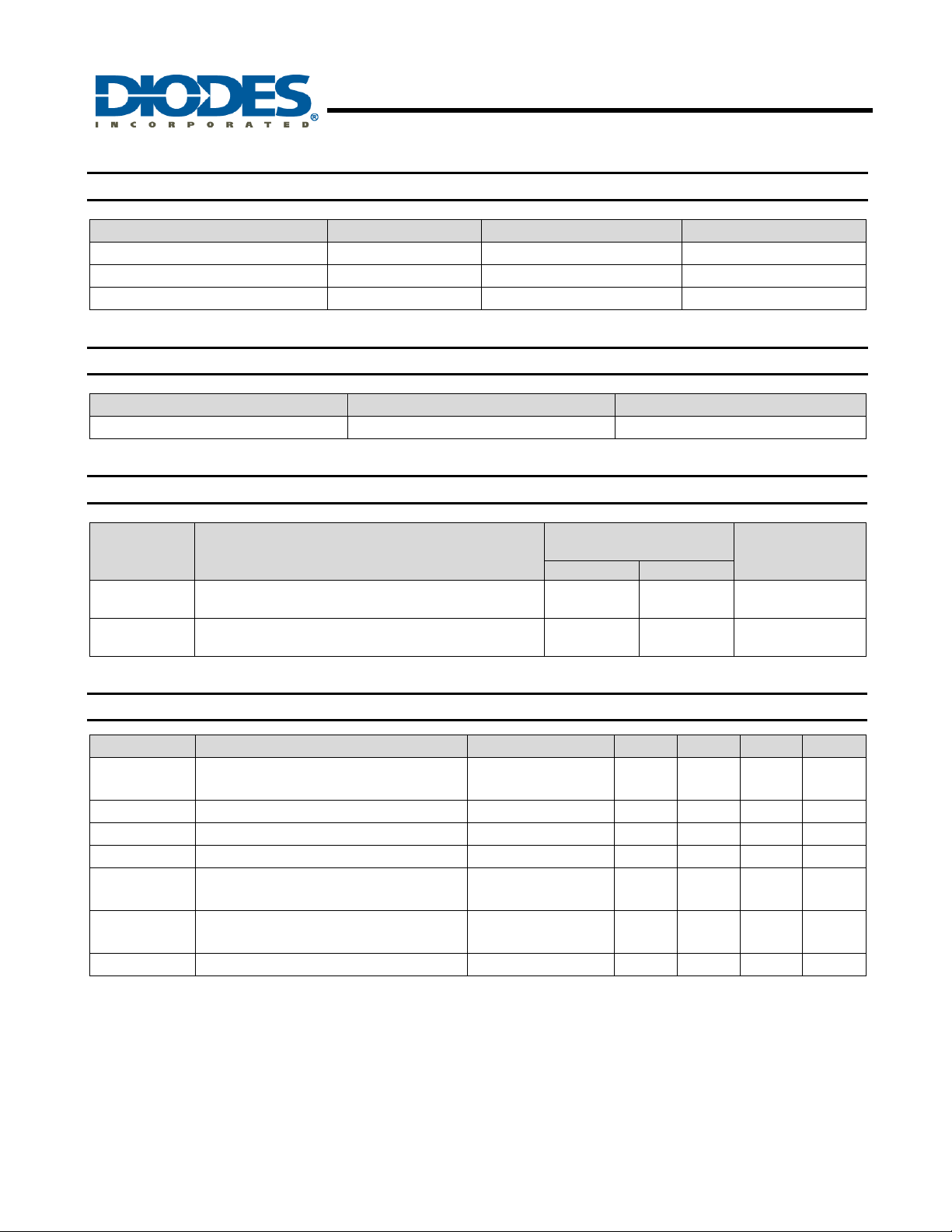
Absolute Maximum Ratings
Parameter Symbol Value Unit
Reverse Current (Note 1) 75 mA
Operating Temperature: C grade T
Storage Temperature T
Notes: 1. Above 72°C this figure should be linearly derated to 15mA @ 125°C
OMP
-55 to +150 °C
STG
Power Dissipation (@T
= 25°C unless otherwise stated)
amb
Package Value Unit
SOT223 2 W
Temperature Dependent Electrical Characteristics
Symbol Parameter
ΔVR
TCVR
Output voltage change over operating temperature
range
Output voltage temperature coefficient
(see Note B)
Electrical Characteristics (@T
Symbol Parameter Conditions Min. Typ. Max. Unit
VR
V
TRIM
TCV
TRIM
IR Operating current range 0.15 75 mA
ton
t
off
e
np-p
RS Slope resistance (see Note C) IR = 0.5mA to 5mA 1.1 3.0 Ω
Output voltage:
1% tolerance
Output voltage adjustment range RT = 100kΩ ±5 %
Change in TCVR with output adjustment 2.5 ppm/°C
Turn-on time
Turn-off time
Output voltage noise
(over the range 0.1 to 10Hz)
= 25°C unless otherwise stated)
amb
Peak to peak
measurement
-40 to +85 °C
Grade C
-40 to 85°C
Typ. Max.
7.5 24.0 mV
15.0 50.0 ppm/°C
IR = 500 µA 3.97 4.01 4.05 V
RL = 1kΩ
50 µV
40
0.3
µs
Unit
ZRT040
Document number: DS33258 Rev. 5 - 2
2 of 5
www.diodes.com
February 2011
© Diodes Incorporated
 Loading...