

Page 1
2.5V LOW POWER PRECISION REFERENCE SOURCE
Description
The ZRT025 is a monolithic integrated circuit providing a
precise stable reference voltage of 2.5V at 500μA.
The circuit features a knee current of 150μA and operation
over a wide range of temperatures and currents.
The ZRT025 is available for surface mount applications. This
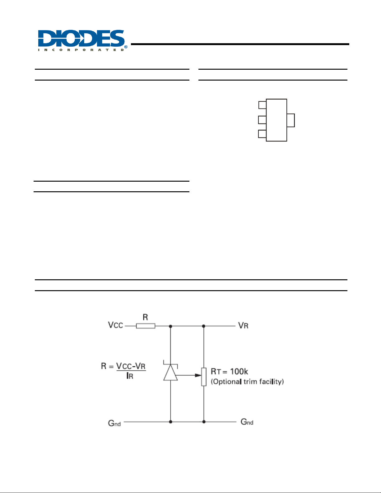
product offers a trim facility whereby the output voltage can
be adjusted as shown in the schematic diagram. This facility
is used when compensating for system errors or setting the
reference output to a particular value. When the trim facility is
not used, the pin should be left open circuit.
Features
• Trimmable output
• Excellent temperature stability
• Low output noise figure
• -40 to 85°C operating temperature range
• 1% initial voltage tolerance
• No external stabilizing capacitor required in most cases
• Low slope resistance
• No derating required at low temperatures
• SOT223 package
Pin Assignments
SOT223
T
RIM
GND
V
R
(Pin 4 floating or
connected to pin 2)
1
2
3
Top View
4
ZRT025
Schematic Diagram
This circuit will allow the reference to be trimmed over a wide range. The device is specified over a ±5% trim range.
ZRT025
Document number: DS33257 Rev. 5 - 2
1 of 5
www.diodes.com
February 2011
© Diodes Incorporated
Page 2
ZRT025
2.5V LOW POWER PRECISION REFERENCE SOURCE
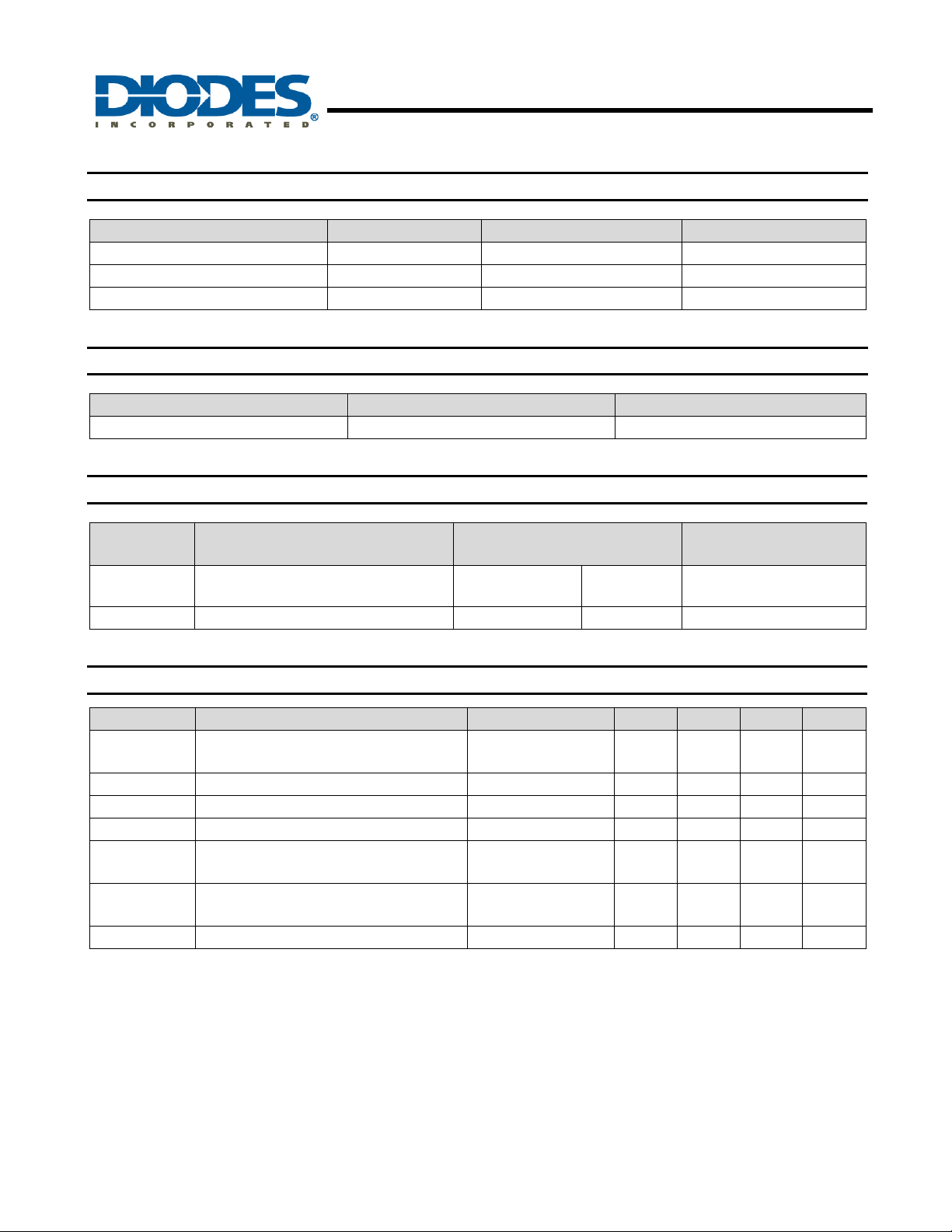
Absolute Maximum Ratings
Parameter Symbol Value Unit
Reverse Current (Note 1) 75 mA
Operating Temperature: C grade T
Storage Temperature T
Notes: 1. Above 72°C this figure should be linearly derated to 25mA @ 125°C
OMP
-55 to +150 °C
STG
Power Dissipation (@T
= 25°C unless otherwise stated)
amb
Package Value Unit
SOT223 2 W
Temperature Dependent Electrical Characteristics
Symbol Parameter
ΔVR
TCVR Output voltage temperature coefficient 15.0 50.0 ppm/°C
Output voltage change over relevant
temperature range
Electrical Characteristics (@T
Symbol Parameter Conditions Min. Typ. Max. Unit
VR
V
TRIM
TCV
TRIM
IR Operating current range 0.15 75 mA
ton
t
off
e
np-p
RS Slope resistance (see note C) IR = 0.5mA to 5mA 0.85 2.0 Ω
Output voltage
1% tolerance
Output voltage adjustment range RT = 100kΩ ±5 %
Change in TCVR with output adjustment 2.5 ppm/°C
Turn-on time
Turn-off time
Output voltage noise
(over the range 0.1 to 10Hz)
= 25°C unless otherwise stated)
amb
Peak to peak
measurement
ZRT025
Document number: DS33257 Rev. 5 - 2
2 of 5
www.diodes.com
-40 to +85 °C
Grade C
-40 to 85°C
2.7 8.8 mV
IR = 500 µA 2.475 2.500 2.525 V
= 1kΩ
R
L
50 µV
10
0.3
Unit
µs
February 2011
© Diodes Incorporated
Page 3
Typical Characteristics
ZRT025
2.5V LOW POWER PRECISION REFERENCE SOURCE
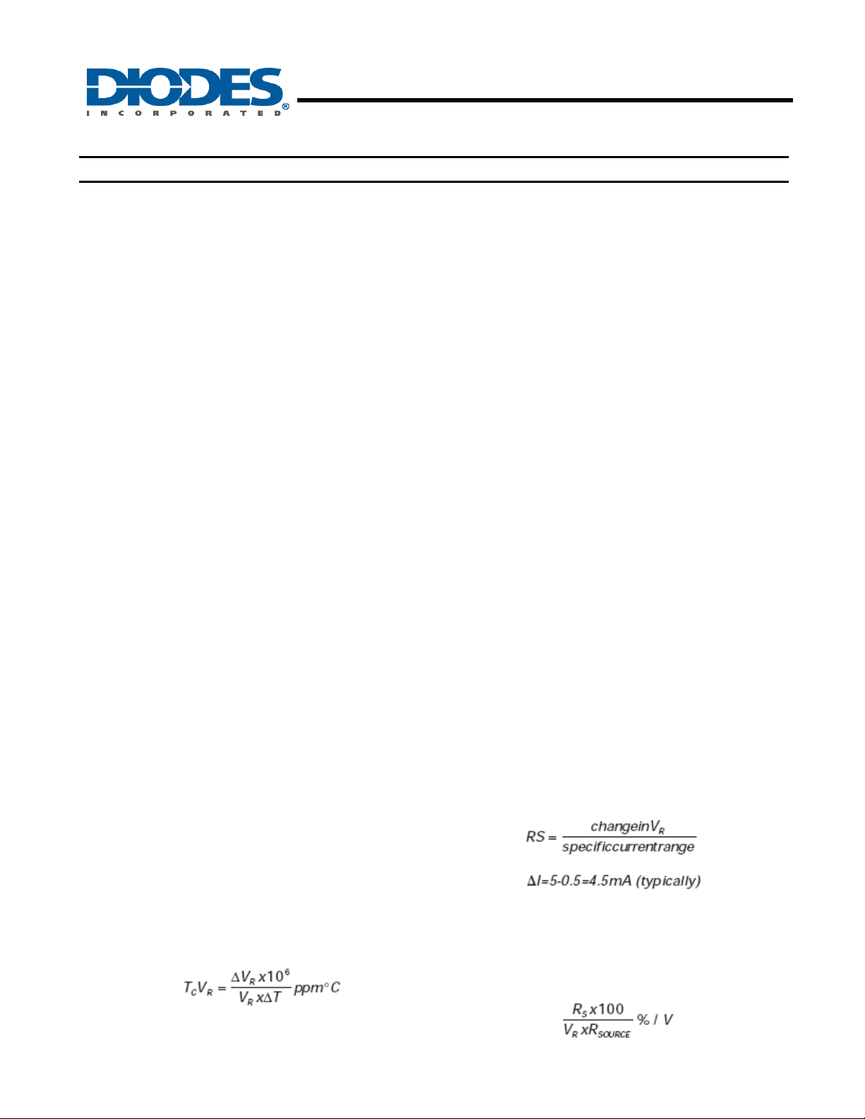
(a) Output change with temperature
The absolute maximum difference between the maximum
output voltage and the minimum output voltage over the
specified temperature range
ΔV
R=VMAX
(b) Output temperature coefficient (T
The ratio of the output change with temperature to the
specified temperature range expressed in ppm/°C
ΔT= Full temperature range
- V
MIN
)
CVR
ZRT025
Document number: DS33257 Rev. 5 - 2
www.diodes.com
(c) Slope resistance (RS)
The slope resistance is defined as :
(d) Line regulation
The ratio of change in output voltage to the change in
input voltage producing it.
3 of 5
February 2011
© Diodes Incorporated
Page 4
ZRT025
2.5V LOW POWER PRECISION REFERENCE SOURCE
Ordering Information
Device Tol %
ZRT025GC1TA 1 -40 to +85 ZRT025C1 7” 12mm 1000
Operating
Temperature
Part Mark
Reel
Size
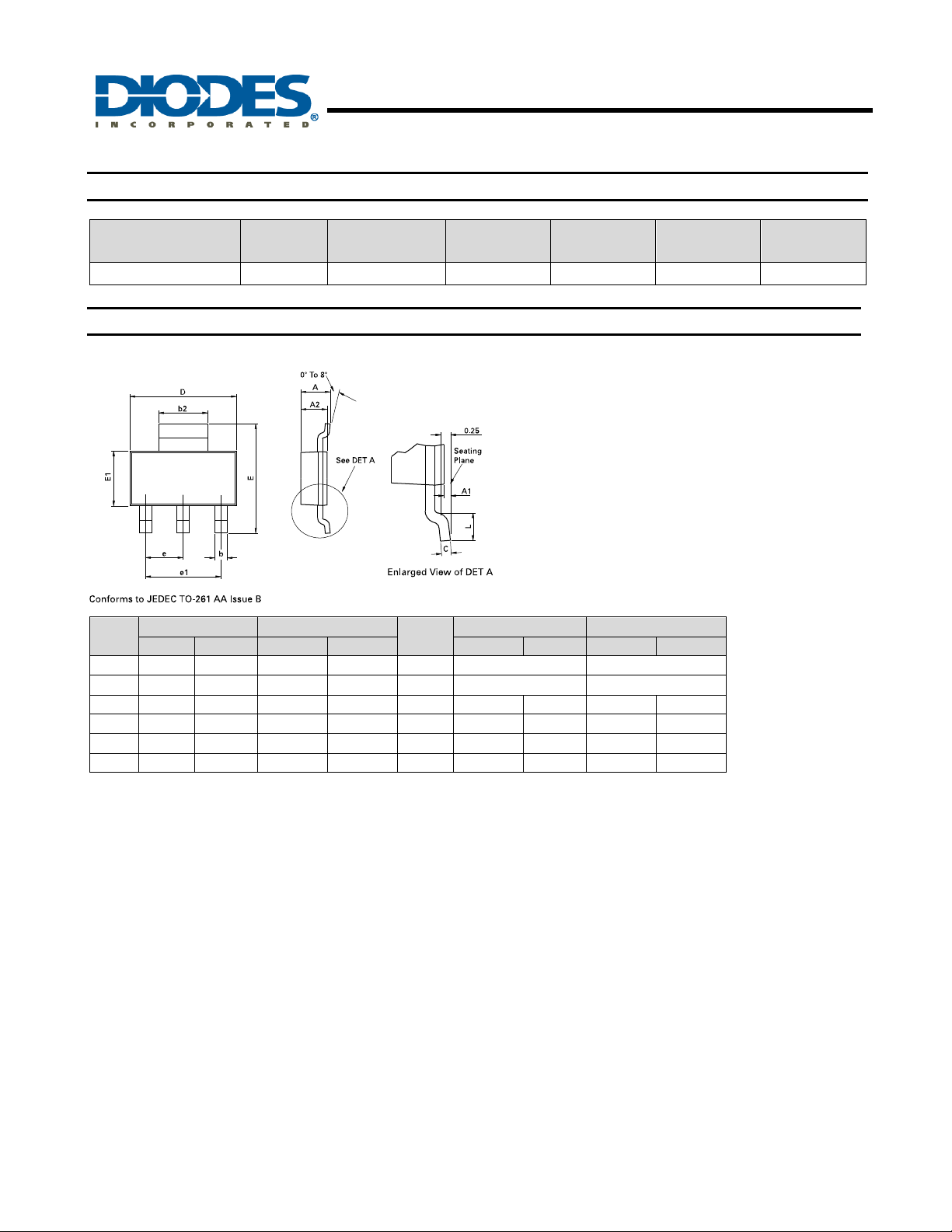
Package Outline Dimensions (All Dimensions in mm)
SOT223
Tape
Width
Quantity
Per Reel
DIM
A - 1.80 - 0.071 e 2.30 BSC 0.0905 BSC
A1 0.02 0.10 0.0008 0.004 e1 4.60 BSC 0.181 BSC
b 0.66 0.84 0.026 0.033 E 6.70 7.30 0.264 0.287
b2 2.90 3.10 0.114 0.122 E1 3.30 3.70 0.130 0.146
C 0.23 0.33 0.009 0.013 L 0.90 - 0.355 D 6.30 6.70 0.248 0.264 - - - - -
Note: Controlling dimensions are in millimeters. Approximate dimensions are provided in inches.
Millimeters Inches
Min Max Min Max Min Max Min Max
DIM
Millimeters Inches
ZRT025
Document number: DS33257 Rev. 5 - 2
4 of 5
www.diodes.com
February 2011
© Diodes Incorporated
Page 5

ZRT025
2.5V LOW POWER PRECISION REFERENCE SOURCE
IMPORTANT NOTICE
DIODES INCORPORATED MAKES NO WARRANTY OF ANY KIND, EXPRESS OR IMPLIED, WITH REGARDS TO THIS
DOCUMENT, INCLUDING, BUT NOT LIMITED TO, THE IMPLIED WARRANTIES OF MERCHANTABILITY A ND FITNESS FOR A
PARTICULAR PURPOSE (AND THEIR EQUIVALENTS UNDER THE LAWS OF ANY JURISDICTION).
Diodes Incorporated and its subsidiaries reserve the right to make modifications, enhancements, improvements, corrections or other
changes without further notice to this document and any product described herein. Diodes Incorporat ed does not assume any liability
arising out of the application or use of this document or any product described herein; neither does Diodes Incorporated convey any
license under its patent or trademark rights, nor the rights of others. A ny Customer or user of this document or products described
herein in such applications shall assume all risks of such use and will agree to hold Diodes Incorporated and all the companies
whose products are represented on Diodes Incorporated website, harml ess ag ai nst all damages.
Diodes Incorporated does not warrant or acc ept any liability whatsoever in respec t of any products purchas ed through unauthorized
sales channel.
Should Customers purchase or use Diodes Incorporated products for any unintended or unauthorized application, Customers shall
indemnify and hold Diodes Incorporated and its representatives harmless agai nst all claims, damages, expenses, and attorney fees
arising out of, directly or indirectly, any claim of personal injury or death ass ociated with such unintended or unauthorized application.
Products described herein may be covered by one or more United Stat es, international or foreign patents pending. Product names
and markings noted herein may also be covered by one or more United States, international or foreign trademarks.
LIFE SUPPORT
Diodes Incorporated products are specifically not authorized for use as critical components in life support devices or systems without
the express written approval of the Chief Executive Officer of Diodes Incorporated. As used herei n:
A. Life support devices or systems are devices or systems which:
1. are intended to implant into the body, or
2. support or sustain life and whose failure to perform when properly used in accordance with instructi ons for us e provided
in the labeling can be reasonably expected to result in significant injury to the user.
B. A critical component is any component in a life support device or syst em whose failure to perform can be reasonably expected
to cause the failure of the life support device or to affect its safety or effectiveness .
Customers represent that they have all necessary expertise in the safety and regulatory ramifications of their life support devices or
systems, and acknowledge and agree that they are solely responsible for all legal, regulatory and safety-related requirements
concerning their products and any use of Diodes Incorporated products in such safety-critical, life support devices or systems,
notwithstanding any devices- or systems-related information or support that may be provided by Diodes Incorporated. Further,
Customers must fully indemnify Diodes Incorporated and its representatives agai nst any damages arising out of the use of Diodes
Incorporated products in such safety-critic al, l ife support devic es or syst ems .
Copyright © 2011, Diodes Incorporated
www.diodes.com
ZRT025
Document number: DS33257 Rev. 5 - 2
5 of 5
www.diodes.com
February 2011
© Diodes Incorporated
 Loading...