

Page 1
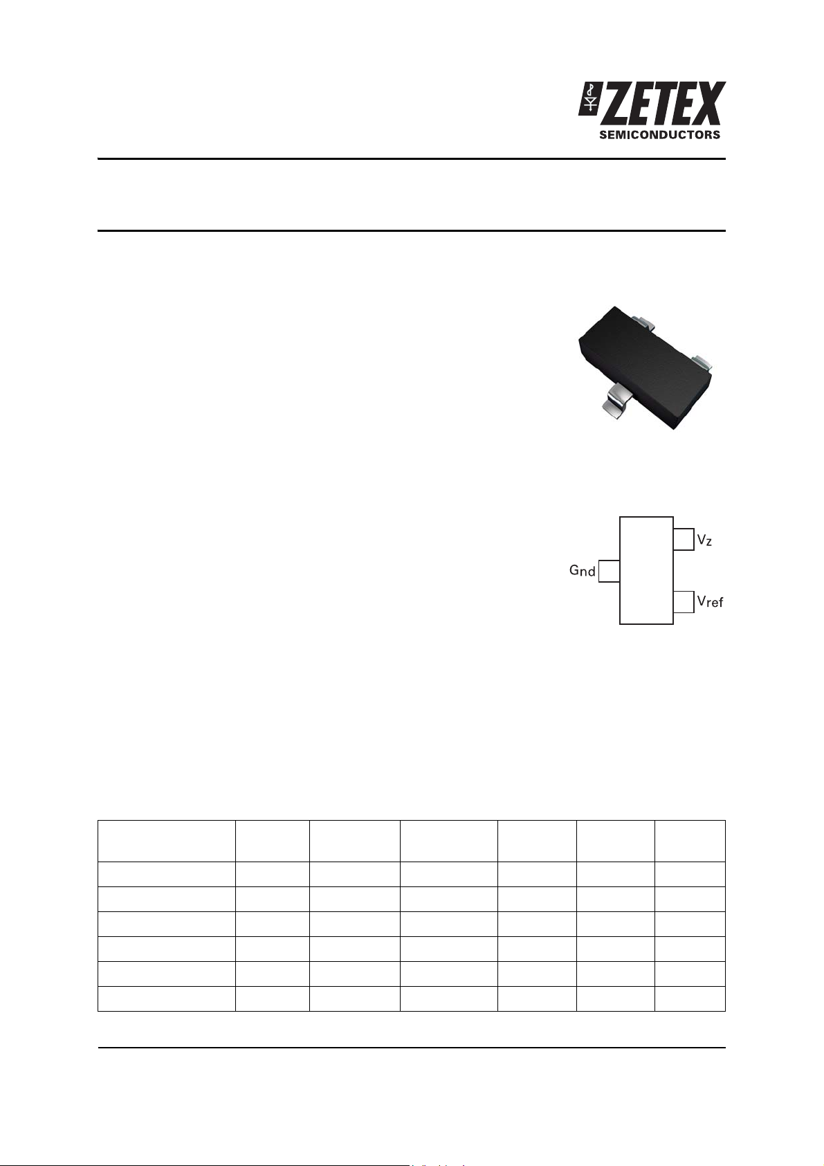
ZR431L
Adjustable precision shunt regulator
Summary
Description
The ZR431L is a three terminal adjustable shunt regulator offering excellent
temperature stability and output current handling capability up to 25mA.
The output voltage may be set to any chosen voltage between 1.24 and
10 volts by selection of two external divider resistors.
The devices can be used as a replacement for zener diodes in many
applications requiring an improvement in zener performance.
The ZR431L is particularly used in the feedback control loop of switch mode
power supplies. In this application the device 1.24 volt reference enables
the generation of low voltage supplies, typically 3.3 volts or 3 volts.
Features
• 2.5% and 1% tolerance
• Max. temperature coefficient 50 ppm/°C
• Temperature compensated for operation over -40 to 85°C
• 100mA to 25mA current sink capability
• Surface mount SOT23 package
Applications
• Switch mode power supplies
• Shunt regulator
• Series regulator
• Voltage monitor
• Over voltage / under voltage protection
Ordering information
Device Pack Part mark Status Quantity
per reel
ZR431LF01TA SOT23 43M Active 3000 7 1
ZR431LF02TA SOT23 43L Active 3000 7 2.5
ZR431LC01STOB TO92 ZR431L01 Obsolete 1500 1
ZR431LC02STOB TO92 ZR431L02 Obsolete 1500 2.5
ZR431LC01L TO92 ZR431L01 Obsolete Loose 1
ZR431LC02L TO92 ZR431L02 Obsolete Loose 2.5
Reel size
(inches)
TOL %
Issue 3 - April 2008 1 www.zetex.com
© Zetex Semiconductors plc 2008
Page 2

ZR431L
Absolute maximum ratings
Parameter Symbol Limit Unit
Cathode voltage V
Cathode current 50 mA
Storage temperature T
Junction temperature T
Z
STG
J
10 V
-55 to 105 °C
-40 to 125 °C
Power dissipation (at T
Package Value Unit
SOT23 330 mW
= 25°C unless otherwise stated)
amb
Recommended operating conditions
Parameter Min. Max.
Cathode voltage V
Cathode current 100A25mA
Operating temperature -40°C 85°C
REF
10V
Issue 3 - April 2008 2 www.zetex.com
© Zetex Semiconductors plc 2008
Page 3
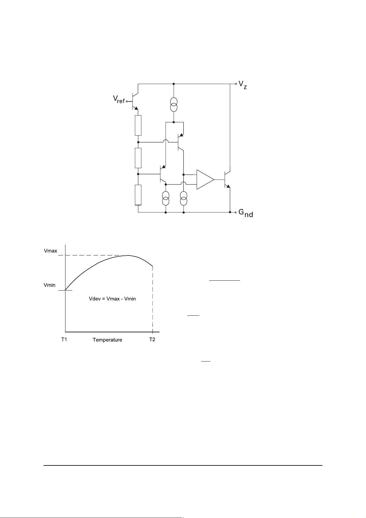
Block diagram
)21(
0
)(
TTV
xV
ppmICVref
ref
dev
−
=
Z
Z
Z
I
V
R
Δ
Δ
=
)
1
1('
R
R
RR
Z
+=
ZR431L
Deviation of reference input voltage, V
the maximum variation of the reference input voltage
over the full temperature range.
The average temperature coefficient of the reference
input voltage, V
is defined as:
ref
, is defined as
dev
100000
The dynamic output impedance, R
When the device is programmed with two external
resistors, R1 and R2, (fig 2), the dynamic output
impedance of the overall circuit, R’, is defined as:
, is defined as:
z
2
Issue 3 - April 2008 3 www.zetex.com
© Zetex Semiconductors plc 2008
Page 4

ZR431L
Z
ref
V
V
Δ
Δ
Electrical characteristics (at T
= 25°C unless otherwise stated)
amb
Parameter Symbol Min. Typ. Max. Unit Conditions
Reference Voltage 2.5%
1.0%
Deviation of Reference
Input Voltage over
V
ref
V
ref
V
dev
1.209
1.228
1.24
1.24
1.271
1.252
VVIL = 10mA (Fig1), VZ = V
4.0 8.0 mV IL = 10mA, VZ = V
Ta = full range (Fig 1)
Temperature
Ratio of the change in
Reference Voltage to the
change in Cathode
0.5 2.0 mV/V
VZ from V
I
= 10mA (Fig2)
Z
Voltage)
Reference Input Current I
Deviation of Reference
Input Current over
Temperature
Minimum Cathode
Current for Regulation
Off-state Current I
ref
⌬I
I
Zmin
Zoff
ref
0.02 0.11 0.4 A R1 = 10k, R2 = O/C,
l
= 10mA (fig2)
L
0.02 0.2 A R1 = 10k, R2 = O/C,
IL = 10mA Ta = full
range (Fig2)
30 100 A
10 30 AVZ = 10V, V
(Fig3)
Dynamic Output
Impedance
R
Z
0.25 2
Ω
VZ = V
ref
= 10mA
I
L
ref
ref
to 10V
ref
= 0V
ref
(Fig1), f = 0Hz,
DC Test circuits
Fig 1 - Test Circuit for V
= V
Z
Fig 2 - Test Circuit for VZ > V
ref
Fig 3 - Test Circuit for Off State
ref
current
Issue 3 - April 2008 4 www.zetex.com
© Zetex Semiconductors plc 2008
Page 5

Typical characteristics
ZR431L
140
130
120
110
100
Reference Current (nA)
90
80
-40 -25 -10 5 20 35 50 65 80 95 110 125
Temperature (°C)
Reference Current v Temperature
26
24
22
20
18
Minimum cathode current (µA)
16
-40 -25 -10 5 20 35 50 65
80 95
Temperature (°C)
Minimum cathode current vs temperature
110 125
0
-1
-2
-3
-4
-5
-6
-7
-8
Change in reference voltage (mV)
-9
0
42
Cathode voltage (V)
6
Change in reference voltage vs Cathode voltage
100
10
V
= V
REF
KA
1
Dynamic Impedance (Ω)
0.1
0.1 1 10 100
IK = 1mA
I
= 10mA
K
Frequency (kHz)
Dynamic impedance vs frequency
0
18
1.244
1.242
1.24
1.238
1.236
Reference voltage (V)
1.234
1.232
-42 -25 -10 5 20 35 50 65 80 95 110 125
Temperature (°C)
Reference voltage vs Temperature
350
300
250
200
150
100
Power dissipation (mW)
50
-40 -25 -10 -5 20 35 50 65 80 95 110 125
Ambient temperature (°C)
Power dissipation derating
Issue 3 - April 2008 5 www.zetex.com
© Zetex Semiconductors plc 2008
Page 6

Application circuits
ZR431L
Issue 3 - April 2008 6 www.zetex.com
© Zetex Semiconductors plc 2008
Page 7

ZR431L
Stability boundary conditions
0
0.01 0.1 1 10 100 1000 10000
5
10
15
20
25
30
Load capacitance (nF)
Cathode current (mA)
Open loop gain vs frequency
0
0 1 10 100
10
20
30
40
50
60
Frequency (kHz)
Open loop gain (dB)
Pulse response
-2.5
0 50 100 150 200 250 300 350 400 450 500
0
2.5
5
Time (μs)
Input Voltage swing (V)
0
1
2
Output voltage swing (V)
V
KA
V
IN
Single
pulse
Repetitive
pulse
Typical characteristics
Issue 3 - April 2008 7 www.zetex.com
© Zetex Semiconductors plc 2008
Page 8

SOT23 Package outline and pad layout details
E
e
L
e1
D
A
c
E1
L1
A1
b
3 leads
mm
inches
0.8
0.031
0.9
0.035
0.95
0.037
2.0
0.079
ZR431L
Dim. Millimeters Inches Dim. Millimeters Inches
Min. Max. Min. Max. Min. Max. Min. Max.
A - 1.12 - 0.044 e1 1.90 NOM 0.075 NOM
A1 0.01 0.10 0.0004 0.004 E 2.10 2.64 0.083 0.104
b 0.30 0.50 0.012 0.020 E1 1.20 1.40 0.047 0.055
c 0.085 0.20 0.003 0.008 L 0.25 0.60 0.0098 0.0236
D 2.80 3.04 0.110 0.120 L1 0.45 0.62 0.018 0.024
e 0.95 NOM 0.037 NOM - - - - -
Note: Controlling dimensions are in millimeters. Approximate dimensions are provided in inches.
Issue 3 - April 2008 8 www.zetex.com
© Zetex Semiconductors plc 2008
Page 9

TO92 Package outline
V
Z
1
2
3
Underside view
G
ND
V
ref
ZR431L
Dim. Millimeters Inches
Min. Max. Min. Max.
A 4.32 4.95 0.170 0.195
b 0.36 0.51 0.014 0.020
E 3.30 3.94 0.130 0.155
e 2.41 2.67 0.095 0.105
e1 1.14 1.40 0.045 0.055
L 12.70 15.49 0.500 0.610
R 2.16 2.41 0.085 0.095
S1 1.14 1.52 0.045 0.060
W 0.41 0.56 0.016 0.022
D 4.45 4.95 0.175 0.195
*° 4° 6° 4° 6°
Note: Controlling dimensions are in millimeters. Approximate dimensions are provided in inches
Issue 3 - April 2008 9 www.zetex.com
© Zetex Semiconductors plc 2008
Page 10

ZR431L
Definitions
Product change
Zetex Semiconductors reserves the right to alter, without notice, specifications, design, price or conditions of supply of any product or
service. Customers are solely responsible for obtaining the latest relevant information before placing orders.
Applications disclaimer
The circuits in this design/application note are offered as design ideas. It is the responsibility of the user to ensure that the circuit is fit for
the user’s application and meets with the user’s requirements. No representation or warranty is given and no liability whatsoever is
assumed by Zetex with respect to the accuracy or use of such information, or infringement of patents or other intellectual property rights
arising from such use or otherwise. Zetex does not assume any legal responsibility or will not be held legally liable (whether in contract,
tort (including negligence), breach of statutory duty, restriction or otherwise) for any damages, loss of profit, business, contract,
opportunity or consequential loss in the use of these circuit applications, under any circumstances.
Life support
Zetex products are specifically not authorized for use as critical components in life support devices or systems without the express written
approval of the Chief Executive Officer of Zetex Semiconductors plc. As used herein:
A. Life support devices or systems are devices or systems which:
1. are intended to implant into the body
or
2. support or sustain life and whose failure to perform when properly used in accordance with instructions for use provided in the
labeling can be reasonably expected to result in significant injury to the user.
B. A critical component is any component in a life support device or system whose failure to perform can be reasonably expected to
cause the failure of the life support device or to affect its safety or effectiveness.
Reproduction
The product specifications contained in this publication are issued to provide outline information only which (unless agreed by the
company in writing) may not be used, applied or reproduced for any purpose or form part of any order or contract or be regarded as a
representation relating to the products or services concerned.
Terms and Conditions
All products are sold subjects to Zetex’ terms and conditions of sale, and this disclaimer (save in the event of a conflict between the two
when the terms of the contract shall prevail) according to region, supplied at the time of order acknowledgement.
For the latest information on technology, delivery terms and conditions and prices, please contact your nearest Zetex sales office.
Quality of product
Zetex is an ISO 9001 and TS16949 certified semiconductor manufacturer.
To ensure quality of service and products we strongly advise the purchase of parts directly from Zetex Semiconductors or one of our
regionally authorized distributors. For a complete listing of authorized distributors please visit: www.zetex.com/salesnetwork
Zetex Semiconductors does not warrant or accept any liability whatsoever in respect of any parts purchased through unauthorized sales channels.
ESD (Electrostatic discharge)
Semiconductor devices are susceptible to damage by ESD. Suitable precautions should be taken when handling and transporting devices.
The possible damage to devices depends on the circumstances of the handling and transporting, and the nature of the device. The extent
of damage can vary from immediate functional or parametric malfunction to degradation of function or performance in use over time.
Devices suspected of being affected should be replaced.
Green compliance
Zetex Semiconductors is committed to environmental excellence in all aspects of its operations which includes meeting or exceeding regulatory requirements with respect to the use of hazardous substances. Numerous successful programs have been implemented to reduce
the use of hazardous substances and/or emissions.
All Zetex components are compliant with the RoHS directive, and through this it is supporting its customers in their compliance with
WEEE and ELV directives.
Product status key:
“Preview” Future device intended for production at some point. Samples may be available
“Active” Product status recommended for new designs
“Last time buy (LTB)” Device will be discontinued and last time buy period and delivery is in effect
“Not recommended for new designs”
“Obsolete” Production has been discontinued
Datasheet status key:
“Draft version” This term denotes a very early datasheet version and contains highly provisional information, which
“Provisional version” This term denotes a pre-release datasheet. It provides a clear indication of anticipated performance.
“Issue” This term denotes an issued datasheet containing finalized specifications. However, changes to
Zetex sales offices
Europe
Zetex GmbH
Kustermann-park
Balanstraße 59
D-81541 München
Germany
Telefon: (49) 89 45 49 49 0
Fax: (49) 89 45 49 49 49
europe.sales@zetex.com
© 2008 Published by Zetex Semiconductors plc
Device is still in production to support existing designs and production
may change in any manner without notice.
However, changes to the test conditions and specifications may occur, at any time and without notice.
specifications may occur, at any time and without notice.
Americas
Zetex Inc
700 Veterans Memorial Highway
Hauppauge, NY 11788
USA
Telephone: (1) 631 360 2222
Fax: (1) 631 360 8222
usa.sales@zetex.com
Asia Pacific
Zetex (Asia Ltd)
3701-04 Metroplaza Tower 1
Hing Fong Road, Kwai Fong
Hong Kong
Telephone: (852) 26100 611
Fax: (852) 24250 494
asia.sales@zetex.com
Corporate Headquarters
Zetex Semiconductors plc
Zetex Technology Park, Chadderton
Oldham, OL9 9LL
United Kingdom
Telephone: (44) 161 622 4444
Fax: (44) 161 622 4446
hq@zetex.com
Issue 3 - April 2008 10 www.zetex.com
© Zetex Semiconductors plc 2008
 Loading...