DIODES ZPU180, ZPU100, ZPU120, ZPU150 Datasheet

Features
Planar Die Construction
·
1.3W Power Dissipation
·
Zener Voltages Available from 100V - 180V
·
Hermetic Glass Package for High Reliability
·
ZPU100 - ZPU180
SILICON POWER ZENER DIODE
A
B
A
D
Mechanical Data
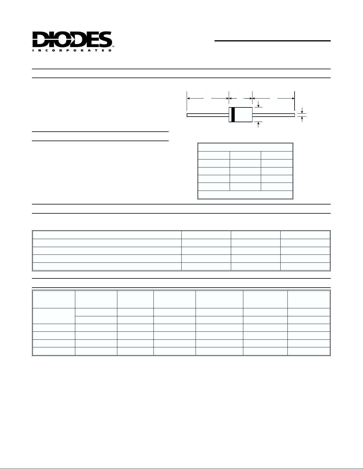
Case: DO-41, Glass
·
Leads: Solderable per MIL-STD-202, Method
·
208
Polarity: Color Band Denotes Cathode
·
Weight: 0.3 grams (approx)
·
Mounting Position: Any
·
Maximum Ratings and Electrical Characteristics
Single phase, half wave, 60Hz, resistive or inductive load.
For capacitive load, derate current by 20%.
Characteristics Symbol Value Unit
Zener Current see Table below
Maximum Power Dissipation (Note 1)
Maximum Thermal Resistance Junction to Ambient Air (Note 1)
Storage and Operating Temperature Range
Electrical Characteristics
Type
ZPU100 88-110 5 300 +.110 75 11.8
ZPU120 107-134 5 330 +.110 90 9.7
ZPU150 130-165 5 360 +.110 112 7.87
ZPU180 160-200 5 380 +.110 134 6.5
Zener
Voltage Range
(Note 2)
VZ@I
ZT
Volts mA Ohms %/°C Volts mA
@ TA= 25°C unless otherwise specified
Test
Current
I
ZT
Maximum
Dynamic
Impedance
ZZT@I
ZT
Dim Min Max
A 25.4 —
B 4.1 5.2
C 0.71 0.86
D 2.0 2.7
@ TA= 25°C unless otherwise specified
———
P
d
R
qJA
T
j,TSTG
Typ. Temperature
Coefficient
@I
DO-41
All Dimensions in mm
1.3 W
130 °C/W
–55 to +200 °C
Minimum
Reverse
Voltage
ZT
VR@ IR= 0.5 µA I
C
Maximum
Zener Current
(Note 1)
ZM
Notes: 1. Valid provided that leads are kept at ambient temperature at a distance of 10mm from case.
2. Tested with pulses tp = 20 ms.
DS21405 Rev.D-3 1 of 2 ZPU100-ZPU180

g
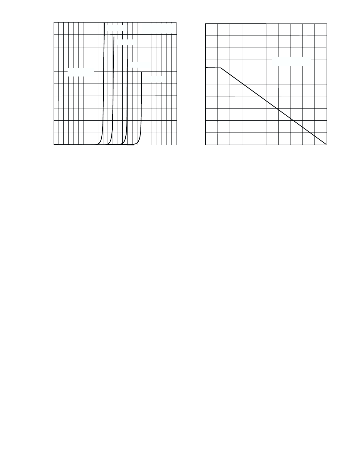
10
ZPU100
g
2
T = 25°C
A
8
6
(See Note 2)
ZPU120
ZPU150
ZPU180
1
4
Z
I , ZENER CURRENT (mA)
2
0
0
Notes: 1. Valid provided that leads are kept at ambient temperature at a distance of 10mm from case.
2. Tested with pulses tp = 20 ms.
50
. 1 Zener Breakdown Characteristics
Fi
100
V , ZENER VOLTAGE (V)
Z
150 200
250
d
P , POWER DISSIPATION, (W)
0
0 100 200
T , Ambient Temperature (ºC)
A
Fi
. 2 Power DeratingCurve
(See Note 1)
DS21405 Rev.D-3 2 of 2 ZPU100-ZPU180
 Loading...