

Page 1
A
f
Description
The ZNBG4003 is a four stage depletion mode FET bias controller
intended primarily for satellite Low Noise Block’s (LNB’s), but its also
suitable for other LNA applications such as those in found in PMR’s
and microwave links. The ZNBG4003 provides each FET with a
negative gate voltage and positive drain voltage with user
programmable drain current.
Product Line o
Diodes Incorporated
ZNBG4003
4 STAGE LNA BIAS CONTROLLER
Pin Assignments
Features
• Four stage FET bias controller
• Operating range of 4.75V to 8.0V
• FET drain voltages set at 2.0V
NEW PRODUCT
• FET drain current selectable from 0 to 15mA
• Allows first and second stage FETs to be run at different
(optimum) drain currents
• FET drain voltages and currents stable over temperature
• FETs protected against overstress during power-up and power-
down.
• Internal negative supply generator allowing single supply
operation (available for external use)
• Low external component count
• Totally Lead-Free & Fully RoHS Compliant (Notes 1 & 2)
• Halogen and Antimony Free. “Green” Device (Note 3)
Notes: 1. No purposely added lead. Fully EU Directive 2002/95/EC (RoHS) & 2011/65/EU (RoHS 2) compliant.
2. See http://www.diodes.com for more information about Diodes Incorporated’s definitions of Halogen- and Antimony-free, "Green" and Lead-free.
3. Halogen- and Antimony-free "Green” products are defined as those which contain <900ppm bromine, <900ppm chlorine (<1500ppm total Br + Cl) and
<1000ppm antimony compounds.
Applications
• Two single type Twin LNB’s
• Twin LNB’s
• Quad LNB’s
• Microwave links
• PMR and Cellular telephone systems
Top view
Bottom view
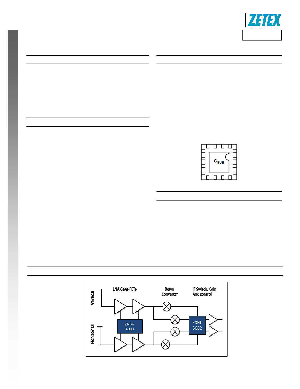
Twin Universal LNB System Diagram
ZNBG4003
Document number: DS35007 Rev. 1 - 2
1 of 6
www.diodes.com
June 2012
© Diodes Incorporated
Page 2
A
f
Device Description
The ZNBG series of devices are designed to meet the bias
requirements of GaAs and HEMT FETs commonly used in
satellite receiver LNBs with a minimum of external components.
The ZNBG4003 provides four FET bias stages, arranged in two
pairs of two. Resistors connected to pins R
FET drain currents of each pair over the range of 0 to 15mA,
allowing input FETs to be biased for optimum noise and amplifier
FETs for optimum gain.
Drain voltages of all stages are set at 2.0V. The drain supplies are
current limited to approximately 5% above the operating currents
set by the Rcal resistors.
Depletion mode FETs require a negative voltage bias supply when
operated in grounded source circuits. The ZNBG4003 includes an
NEW PRODUCT
integrated switched capacitor DC-DC converter generating a
regulated output of -2.5V to allow single supply operation.
These devices are unconditionally stable over the full working
temperature with the FETs in place, subject to the inclusion of the
CAL
1 and R
Typical Application Circuit
2 set the
CAL
Product Line o
Diodes Incorporated
ZNBG4003
recommended gate and drain capacitors. These ensure RF
stability and minimal injected noise.
It is possible to use less than the devices full complement of FET
bias controls, unused drain and gate connections can be left open
circuit without affecting operation of the remaining bias circuits.
To protect the external FETs the circuits have been designed to
ensure that, under any conditions including power up/down
transients, the gate drive from the bias circuits cannot exceed -3V.
Additionally each stage has its own individual current limiter.
Furthermore if the negative rail experiences a fault condition, such
as overload or short circuit, the drain supply to the FETs will shut
down avoiding excessive current flow.
To minimise PCB space ZNBG4003 is packaged in the 16 pin
3mm x 3mm QFN package.
Device operating temperature is -40°C to +85°C to suit a wide
range of environmental conditions.
ZNBG4003
Document number: DS35007 Rev. 1 - 2
www.diodes.com
2 of 6
June 2012
© Diodes Incorporated
Page 3

A
f
Product Line o
Diodes Incorporated
ZNBG4003
Absolute Maximum Ratings (@T
= +25°C, unless otherwise specified.) (Note 5)
A
Parameter Rating Unit
Supply Voltage -0.6 to +10 V
Supply Current 80 mA
Power Dissipation 500 mW
Opereating Temperature Range -40 to +85 °C
Storage Temerature Range -40 to +150 °C
Electrical Characteristics
(@ T
NEW PRODUCT
Notes: 4. The two VCC pins are internally connected, only one of the pins needs to be powered for the device to function. See applications section for further
information.
5. ESD sensitive, handling precautions are recommended.
6. The negative bias voltages are generated on-chip using an internal oscillator. Two external capacitors, C
purpose.
7. The package (QFN1633) exposed pad must either be connected to Csub or le ft open circuit.
8. Noise voltage measurements are made with FETs and gate and drain capacitors of value 10nF in place. Noise voltages are not measured in production.
ZNBG4003
Document number: DS35007 Rev. 1 - 2
= +25°C, VCC = 5.0V (Note 1), R
AMB
CAL
1 = R
2 = 39k (setting ID to 10mA) unless otherwise specified.)
CAL
Symbol Parameter Conditions Min Typ Max Unit
VCC
ICC
I
CC(L)
V
CSUB
V
CSUB(L)
F
OSC
Gate Characteristics
Gate (G1 to G4)
IG
V
G(L)
V
G(H)
Drain Characteristics
Drain (D1 to D4)
ID Current Range 0 15 mA
I
D(OP)
V
D(OP)
dID/dVCC Δ ID vs VCC V
dID/d
dID/dVCC Δ VD vs VCC VCC = 5.0V to 8.0V 0.08 %/V
dID/d
Output Noise (Note 8)
V
D(NOISE)
V
G(NOISE)
Operating Voltage Range (Note 4) 4.75 8.0 V
Supply Current
I
Substrate Voltage (Note 6,7)
I
Oscillator Frequency 150 240 600 kHz
ID1 = ID2 = ID3 = ID4 = 0
= ID2 = ID3 = ID4 = 10mA
D1
I
= 0
CSUB
= -100µA
CSUB
1.8 4.5 mA
43 45
-3.0 -2.65 -2.0 V
-2.55 -1.9 V
Current Range -100 +500 µA
Voltage Low
Voltage High
ID = 12mA, IG = 10µA
ID = 8mA, IG = 0
-3.0 -2.5 -2.0 V
0 0.7 1.0 V
Current Operating Standard Application Circuit 8 10 12.5 mA
Voltage Operating ID = 10mA 1.8 2.0 2.2 V
= 5.0V to 8.0V 1.2 %/V
CC
Δ ID vs TOP T
TOP
Δ VD vs TOP T
TOP
Drain Voltage
Gate Voltage
= -40°C to +85°C 0.09 %/°C
OP
= -40°C to +85°C 110 ppm/°C
OP
C
GRATE-GND
C
DRAIN-GND
C
GRATE-GND
C
DRAIN-GND
= 10nF,
= 10nF
= 10nF,
= 10nF
0.02 Vpk-pk
0.005 Vpk-pk
NB
and C
of value 47nF are required for this
SUB
3 of 6
www.diodes.com
© Diodes Incorporated
June 2012
Page 4

A
f
5
R
CUR
RENT
Typical Characteristics (measured @ T
1
10
(mA)
5
AIN
D
= +25°C, VCC = 5.0V)
AMB
Product Line o
Diodes Incorporated
ZNBG4003
NEW PRODUCT
0
Drain Curr ent vs. R
100 100010
R
CAL
CAL
Application Information
Above is a partial applications circuit for the ZNBG4003 showing
all external components needed for biasing one of the four FET
stages available. Each bias stage is provided with a gate and
drain pin. The drain pin provides a regulated 2.0V supply that
includes a drain current monitor. The drain current taken by the
external FET is compared with a user selected level, generating a
signal that adjusts the gate voltage of the FET to obtain the
required drain current. If for any reason, an attempt is made to
draw more than the user set drain current from the drain pin, the
drain voltage will be reduced to ensure excess current is not
taken. The gate pin drivers are also current limited.
The bias stages are split up into two pairs, with the drain current of
each pair set by an external R
currents of stages 1 and 3, whilst R
stages 2 and 4. This allows the optimisation of drain currents for
differing tasks such as input stages where noise can be critical
and later amplifier stages where gain may be more important.
A graph showing the relationship between the value of R
is provided in the Typical Characteristics section of this datasheet.
resistor. R
CAL
2 sets the drain currents of
CAL
ZNBG4003
Document number: DS35007 Rev. 1 - 2
1 sets the drain
CAL
CAL
and ID
www.diodes.com
The ZNBG4003 includes a switched capacitor DC-DC converter
that is used to generate the negative supply required to bias
depletion mode FETs used in common source circuit configuration
as shown above. This converter uses two external capacitors, C
the charge transfer capacitor and C
capacitor. The circuit provides a regulated -2.5V supply both for
gate driver use and for external use if required (for extra discrete
bias stages, mixer bias, local oscillator bias etc.). The -2.5V
supply is available from the C
If any bias stages are not required, their gate and drain pins may
be left open circuit. If all bias stages associated with an R
resistor are not required, then this resistor may be omitted.
To ease PCB layout, the pinout for the ZNBG4003 includes two
V
pins. These pins are internally connected so only one of the
CC
pins needs to be powered for the device to function. It is probable
that the extra pin will help avoid the need for trace cross-over
components or ground plane disruption from reverse side PCB
links. Note that the exposed pad of the package must be either left
floating or connected to C
4 of 6
SUB
SUB
.
pin.
the output reservoir
SUB
NB
CAL
June 2012
© Diodes Incorporated
Page 5

A
f
Ordering Information
Part Number Packaging
ZNBG4003JA16TC QFN1633 3000/Tape & Reel TC
Marking Information
NEW PRODUCT
Package Outline Dimensions (All dimensions in mm.)
Quantity Part Number Suffix
ZNBG
4003
YYWW
Product Line o
Diodes Incorporated
ZNBG4003
13” Tape & Reel
Pin 1
Part Name
Date Code
Year/Week
QFN16 3x3
Dim Min Max
A 0.55 0.65
A1 0.00 0.05
A3 0.15 Typ
b 0.18 0.28
D 2.95 3.05
D2 1.40 1.60
e 0.50 BSC
E 2.95 3.05
E2 1.40 1.60
L 0.35 0.45
Z 0.625 Typ
All Dimensions in mm
ZNBG4003
Document number: DS35007 Rev. 1 - 2
5 of 6
www.diodes.com
June 2012
© Diodes Incorporated
Page 6

A
f
Product Line o
Diodes Incorporated
ZNBG4003
DIODES INCORPORATED MAKES NO WARRANTY OF ANY KIND, EXPRESS OR IMPLIED, WITH REGARDS TO THIS DOCUMENT,
INCLUDING, BUT NOT LIMITED TO, THE IMPLIED WARRANTIES OF MERCHANTABILITY AND FITNESS FOR A PARTICULAR PURPOSE
(AND THEIR EQUIVALENTS UNDER THE LAWS OF ANY JURISDICTION).
Diodes Incorporated and its subsidiaries reserve the right to make modifications, enhancements, improvements, corrections or other changes
without further notice to this document and any product described herein. Diodes Incorporated does not assume any liability arising out of the
application or use of this document or any product described herein; neither does Diodes Incorporated convey any license under its patent or
trademark rights, nor the rights of others. Any Customer or user of this document or products described herein in such applications shall assume
all risks of such use and will agree to hold Diodes Incorporated and all the companies whose products are represented on Diodes Incorporated
website, harmless against all damages.
Diodes Incorporated does not warrant or accept any liability whatsoever in respect of any products purchased through unauthorized sales channel.
Should Customers purchase or use Diodes Incorporated products for any unintended or unauthorize d application, Customers shall indemnify and
hold Diodes Incorporated and its representatives harmless against all claims, damages, expenses, and attorney fees arising out of, directly or
indirectly, any claim of personal injury or death associated with such unintended or unauthorized application.
Products described herein may be covered by one or more United States, international or foreign patents pending. Product names and markings
noted herein may also be covered by one or more United States, international or foreign trademarks.
NEW PRODUCT
Diodes Incorporated products are specifically not authorized for use as critical components in life support devices or systems without the express
written approval of the Chief Executive Officer of Diodes Incorporated. As used herein:
A. Life support devices or systems are devices or systems which:
1. are intended to implant into the body, or
labeling can be reasonably expected to result in significant injury to the user.
B. A critical component is any component in a life support device or system whose failure to perform can be reasonably expected to cause the
failure of the life support device or to affect its safety or effectiveness.
Customers represent that they have all necessary expertise in the safety and regulatory ramifications of their life support devices or systems, and
acknowledge and agree that they are solely responsible for all legal, regulatory and safety-related requirements concerning their products and any
use of Diodes Incorporated products in such safety-critical, life support devices or systems, notwithstanding any devices- or systems-related
information or support that may be provided by Diodes Incorporated. Further, Customers must fully indemnify Diodes Incorporated and its
representatives against any damages arising out of the use of Diodes Incorporated products in such safety-critical, life support devices or systems.
Copyright © 2012, Diodes Incorporated
www.diodes.com
2. support or sustain life and whose failure to perform when properly used in accordance with instructions for use provided in the
IMPORTANT NOTICE
LIFE SUPPORT
ZNBG4003
Document number: DS35007 Rev. 1 - 2
6 of 6
www.diodes.com
June 2012
© Diodes Incorporated
 Loading...