A
Product Line o
f
Diodes Incorporated
ZNBG3118
LNA GaAs FET BIAS CONTROLLER WITH POLARIZATION AND BA ND SELECT
Summary
The ZNBG3118 is a bias and control solution designed fo r Satellite Low Noise Blocks (LNB’s). Providing three bias stages to
power control and protect the GaAs or HEMT FET low noise amplifier’s (L NA’s). The ZNBG3118 integrates an accurate voltage
detector to select the LNB polarisation channel and an advanced tone detector to select the local oscillator (LO) for band
switching.
Features
• Provides bias for up to three GaAs and HEMT FETs
• Dynamic FET protection and temperature compensation
• Drain current set by external resistor
• Regulated negative rail generator requires only 2 external
capacitors
• Accurate voltage detector and polarisation switch for
LNB’s
• 22kHz tone detection for band switching with rejection of
NEW PRODUCT
unwanted signals
• Band switch supports both Discrete, MIMIC and PLL
local oscillators
• Compliant with ASTRA control specifications
• Low current for power efficient systems
• Wide operating supply range of 3.3V to 8V
Application
• Single Output LNB’s
• Two single type twin LNB’s
• Low power LNB’s
• PLL Single LNB’s
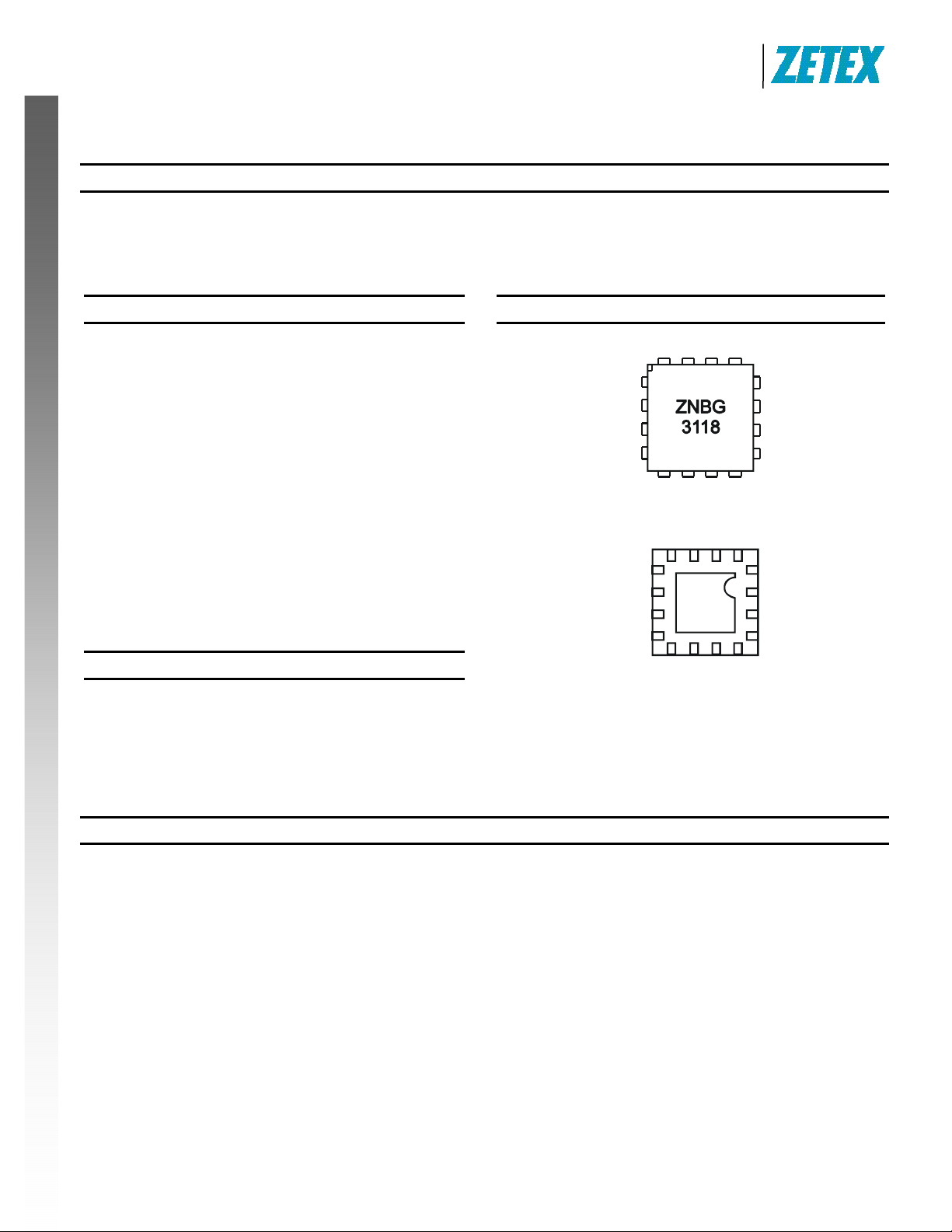
Pin Assignments
G1
GND
C
NB1
C
NB2
D12
G2
G3
IN
CAL
F
SUB
R
C
Top View
C
SUB
Bottom View
D3
LB
HB
V
CC
L
OV
POL
V
Single Universal LNB System Diagram
ZNBG3118
Document number: DS32049 Rev. 2 - 2
1 of 10
www.diodes.com
February 2010
© Diodes Incorporated

A
f
Device Description
The ZNBG series of devices are designed to meet the bias
requirements of GaAs and HEMT FETs commonly used i n
satellite receiver LNBs with a minimum of external
components.
With the addition of two capacitors and a resistor the devices
provide drain voltage and current control for three external
grounded source FETs, generating the regulated negative
rail required for FET gate biasing whilst operating from a
single supply. This negative bias, at -2.5 volts, can also be
used to supply other external circuits.
The ZNBG3118 includes bias circuits to drive up to three
external FETs. The voltage applied to the V
determines which one of first two FETs is operational, the
third FET is permanently active. This feature is normally
used as an LNB polarisation switch to select the required
polarisation. Specific to Universal LNB applications is the
oscillator band select. This is achieved by detecting a 22kHz
tone which enables or disables the relevant local oscillator.
NEW PRODUCT
The ZNBG3118 has been designed to control various
oscillators and down converter designs including Discrete
(Bi-polar or MOSFET), MIMIC oscillators and IF amplifier /
down-converters IC’s with logic enabled phase lock loop
(PLL) oscillators.
The ZNBG3118 has been designed to cope with DiS EqC™
ready set top boxes and rejects transients from channel
switching.
POL
pin
Product Line o
Diodes Incorporated
ZNBG3118
Drain current setting of the ZNBG3118 is user selectable over
the range 0 to 15mA, achieved with addition of a single
resistor. The drain voltage for all the FET’s is set internally to
2 volts. To minimise the pin out and package size FET 1 and
FET 2 share a common drain pin.
These devices are unconditionally stable ov er the full working
temperature with the FETs in place, subject to the i nclusion of
the recommended gate and drain capacitors. These ensure
RF stability and minimal injected noise.
It is possible to use less than the devices full complement of
FET bias controls, unused drain and gate connections can be
left open circuit without affecting operation of the remaining
bias circuits.
To protect the external FETs the circuits have been designed
to ensure that, under any conditions including po wer up/down
transients, the gate drive from the bias circuits cannot exceed
-3V. Additionally each stage has its own individual current
limiter. Furthermore if the negative rail experiences a fault
condition, such as overload or short circuit, the drain supply to
the FETs will shut down avoiding excessive current flow.
To minimise PCB space ZNBG3118 is packaged i n the 16 pin
3mm x 3mm QFN package.
Device operating temperature is -40 to 85°C to suit a wide
range of environmental conditions.
ZNBG3118
Document number: DS32049 Rev. 2 - 2
2 of 10
www.diodes.com
February 2010
© Diodes Incorporated

A
Product Line o
f
V
Diodes Incorporated
Maximum Ratings
Parameter Rating Unit
Supply Voltage -0.6 to +12 V
Supply Current 100 mA
Power Dissipation 500 mW
VPOL Input Voltage 25 Continuous V
Operating Temperature Range -40 to +85 °C
Storage Temperature Range -40 to +150 °C
Electrical Characteristics Measured at Tamb = 25°C, Vcc = 5V, Rcal = 39k (setting Id to 10mA) unless otherwise specified.
ZNBG3118
Parameter Conditions
Supply Voltage
Operating Range
Supply Current Id1 = Id2 = Id3 = 0 1.5 2.5 mA
NEW PRODUCT
Substrate Voltage (Internally generated), Isub=0 -3.0 -2.5 -2.0 V
Oscillator Freq. 150 270 800 kHz
pol Input
Current Vpol = 14.75V (Applied via a 10k resistor) 30 42 52.5 uA
V Threshold (Applied via a 10k resistor) 14.0 14.75 15.5 V
Switching Speed 100 us
Gate characteristics
Gate 1 Output
Voltage Off Id12 = 0, Vpol = 14V, Ig1 = 0 -3.0 -2.5 -2.0 V
Voltage Low Id12 = 12mA, Vpol = 15.5V, Ig1 = -10uA -3.0 -2.5 -2.0 V
Voltage High Id12 = 8mA, Vpol = 15.5V, Ig1 = 0 0.4 0.75 1.0 V
Gate 2 Output
Voltage Off Id12 = 0, Vpol = 15.5V, Ig2 = 0 -3.0 -2.5 -2.0 V
Voltage Low Id12 = 12mA, Vpol = 14V, Ig2 = -10uA -3.0 -2.5 -2.0 V
Voltage High Id12 = 8mA, Vpol = 14V, Ig2 = 0 0.4 0.75 1.0 V
Gate 3 Output
Voltage Low Id3 = 12mA, Ig3 = -10uA -3.0 -2.5 -2.0 V
Voltage High Id3 = 8mA, Ig3 = 0 0.4 0.75 1.0 V
Drain characteristics
Drain 12 Output
Voltage High 1 Id12 = 10mA, Vpol = 15.5V 1.8 2.0 2.2 V
Voltage High 2 Id12 = 10mA, Vpol = 14V 1.8 2.0 2.2 V
Drain 3 Output
Voltage High Id3 = 10mA 1.8 2.0 2.2 V
Drains 12 and 3
delta Vd vs Vcc Vcc = 3.3 to 8V 0.5 %/V
delta Vd vs Tj Tj = -40 to +85°C 50 ppm
D1,2 and 3
Current Range (Set by Rcal) 0 15 mA
Current 8 10 12 mA
delta Id vs Vcc Vcc = 3.3 to 8V 2.5 %/V
delta Id vs Tj Tj = -40 to +85°C 0.05 %/°C
+/-5% Supply tolerance permitted 3.3 8.0 V
Id1 = 0, Id2 = Id3 = 10mA, Vpol = 15.5V 22 24 mA
Id2 = 0, Id1 = Id3 = 10mA, Vpol = 14V 22 24 mA
Id1 = Id2 = Id3 = 0, Ilb = 10mA 12 14 mA
Id1 = Id2 = Id3 = 0, Ihb = 10mA 12 14 mA
Isub = -200uA -2.0 V
Min Typ. Max
Limits
Units
ZNBG3118
Document number: DS32049 Rev. 2 - 2
3 of 10
www.diodes.com
February 2010
© Diodes Incorporated
 Loading...