Diodes ZNBG3114 User Manual

FET BIAS CONTROLLER WITH POLARISATION
SWITCH AND TONE DETECTION
ISSUE 1 - OCTOBER 1998
ZNBG3113
ZNBG3114
DEVICE DESCRIPTION
The ZNBG series of devices are designed to
meet the bias requirements of GaAs and
HEMT FETs commonly used in satellite
receiver LNBs, PMR cellular telephones etc.
with a minimum of external components.
With the addition of two capacitors and a
resistor the devices provide drain voltage and
current control for three external grounded
source FETs, generating the regulated
negative rail required for FET gate biasing
whilst operating from a single supply. This
negative bias, at -3 volts, can also be used to
supply other external circuits.
The ZNBG3113/14 includes bias circuits to
drive up to three external FETs. A control
input to the device selects either one of two
FETs as operational, the third FET is
permanently active. This feature is
particularly used as an LNB polarisation
switch. Also specific to LNB applications is
the 22kHz tone detection and logic output
feature which is used to enable high and low
band frequency switching.
The facility to control the tone switching
delay is provided. This allows the rejection
of other lower frequency tones tat may be
present in multiple LNB applications.
FEATURES
Provides bias for GaAs and HEMT FETs
•
Drives up to three FETs
•
Dynamic FET protection
•
Drain current set by external resistor
•
Regulated negative rail generator
•
requires only 2 external capacitors
Choice in drain voltage
•
Wide supply voltage range
•
Polarisation switch for LNBs
•
22KHz tone detection for band
•
switching
Programmable tone delay
•
Compliant with ASTRA control
•
specifications
QSOP surface mount package
•
Drain current setting of the ZNBG3113/14 is
user selectable over the range 0 to 15mA, this
is achieved with addition of a single resistor.
The series also offers the choice of drain
voltage to be set for the FETs, the 3113 gives
2.2 volts drain whilst the 3114 gives 2 volts.
These devices are unconditionally stable
over the full working temperature with the
FETs in place, subject to the inclusion of the
recommended gate and drain capacitors.
These ensure RF stability and minimal
injected noise.
It is possible to use less than the devices full
complement of FET bias controls, unused
drain and gate connections can be left open
circuit without affecting operation of the
remaining bias circuits.
To protect the external FETs the circuits have
been designed to ensure that, under any
conditions including power up/down
transients, the gate drive from the bias
circuits cannot exceed the range -3.5V to 1V.
Furthermore if the negative rail experiences
a fault condition, such as overload or short
circuit, the drain supply to the FETs will shut
down avoiding excessive current flow.
The ZNBG3113/14 are available in QSOP20
for the minimum in device size. Device
operating temperature is -40 to 70°C to suit
a wide range of environmental conditions.
APPLICATIONS
Satellite receiver LNBs
•
Private mobile radio (PMR)
•
Cellular telephones
•
4-123
ZNBG3113
ZNBG3114
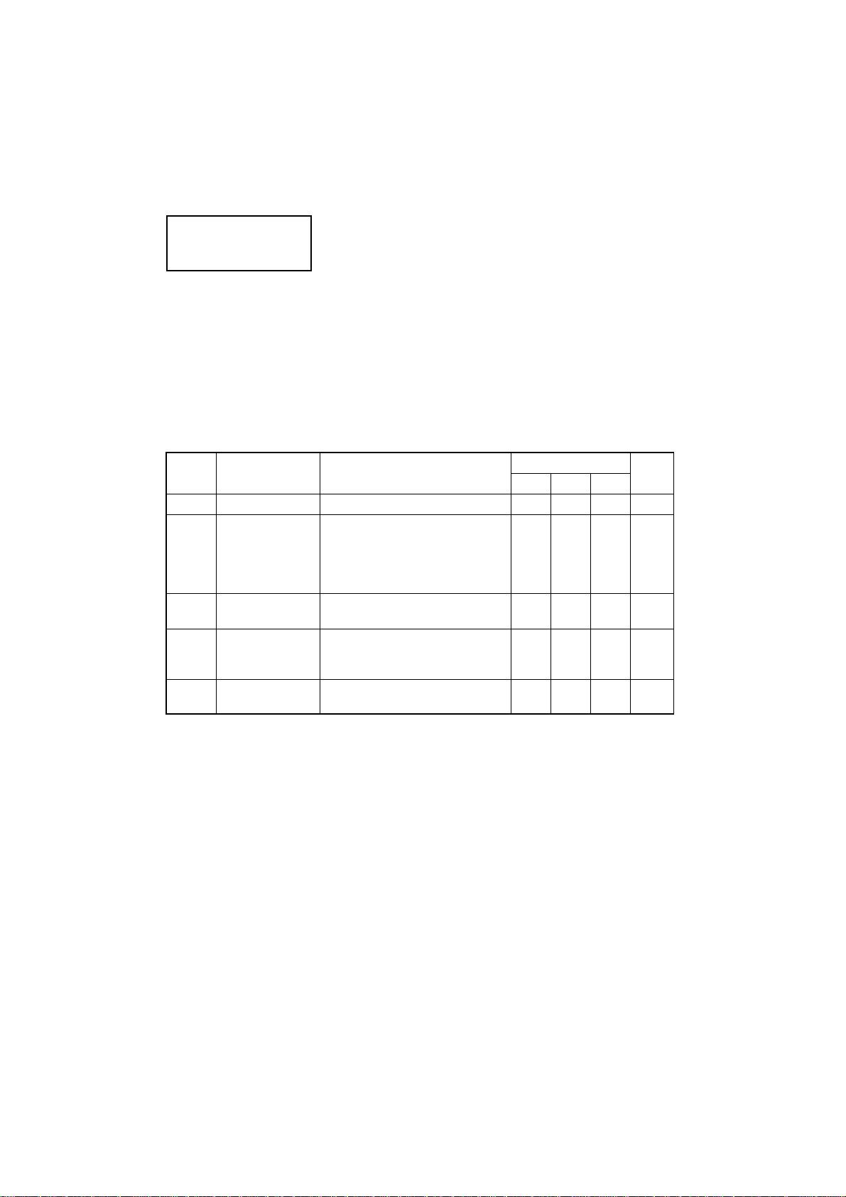
ABSOLUTE MAXIMUM RATINGS
Supply Voltage -0.6V to 12V
Supply Current 100mA
Input Voltage (V
Drain Current (per FET) 0 to 15mA
(set by R
CAL
Operating Temperature -40 to 70°C
Storage Temperature -50 to 85°C
) 25V Continuous
POL
)
Power Dissipation (T
amb
= = 25°C)
QSOP20 500mW
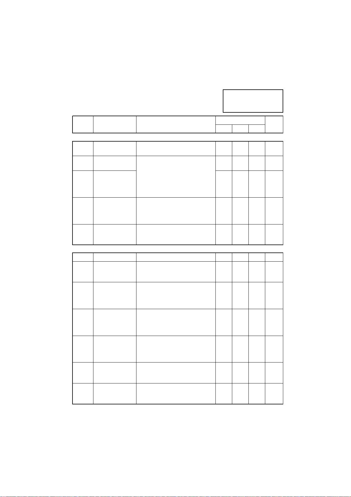
ELECTRICAL CHARACTERISTICS. TEST CONDITIONS
(Unless otherwise stated):T
SYMBOLPARAMETER CONDITIONS
V
I
CC
V
E
E
f
O
Supply Voltage 5 10 V
CC
Supply Current ID1 to ID3=0
I
I
I
I
Substrate Voltage (Internally generated) I
SUB
Output Noise
ND
NG
Drain Voltage
Gate Voltage
C
C
Oscillator
Frequency
= = 25°C,VCC=5V,ID=10mA (R
amb
=0,ID2 to ID3=10mA, V
D1
=0,ID1 to ID3=10mA, V
D2
=0, ILB=10mA
D1 to ID3
=0, IHB=10mA
D1 to ID3
I
=4.7nF, CD=10nF
G
=4.7nF, CD=10nF
G
POL
POL
SUB
SUB
=14V
=15.5V
=0
=-200µA
=33kΩΩ)
CAL
LIMITS
UNITS
MIN. TYP. MAX.
15
mA
35
mA
35
mA
45
mA
45
mA
-3.5 -3.0 -2.5
-2.4VV
0.02
Vpkpk
0.005
Vpkpk
200 350 800 kHz
4-124
ZNBG3113
ZNBG3114
SYMBOLPARAMETER CONDITIONS
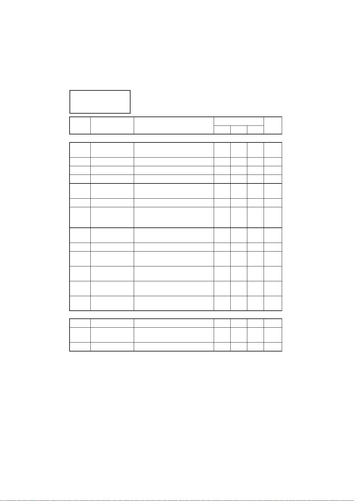
GATE CHARACTERISTICS
I
GO
V
V
V
V
V
V
V
V
G1O
G1L
G1H
G2O
G2L
G2H
G3L
G3H
Output Current
Range
Output Voltage
Gate 1 Off
Low
High
Output Voltage
Gate 2 Off
Low
High
Output Voltage
Gate 3 Low
High
V
I
Dx
POL
(mA) (V) (µµA)
=0 V
I
D1
I
D1
I
D1
I
D2
I
D2
I
D2
I
D3
I
D3
POL
=12 V
POL
=8 V
POL
=0 V
POL
=12 V
POL
=8 V
POL
=12 I
=8 I
DRAIN CHARACTERISTICS
I
DI
DI
V
V
V
DV
DV
I
I
D
L1
L2
Current 8 10 12 mA
Current Change
DV
DT
D1
with V
with T
Drain 1 Voltage:
CC
j
VCC= 5 to 10V
=-40 to +70°C
T
j
High
=10mA, V
I
D1
I
=10mA, V
D1
D2
ZNBG3113
ZNBG3114
Drain 2 Voltage:
High
=10mA, V
I
D2
=10mA, V
I
D2
D3
ZNBG3113
ZNBG3114
Drain 3 Voltage:
High
ZNBG3113
ZNBG3114
=10mA, V
I
D3
=10mA, V
I
D3
Voltage Change
DV
DT
with V
with T
CC
j
VCC= 5 to 10V
=-40 to +70°C
T
j
Leakage Current
Drain 1
Drain 2
V
D1
V
D2
=0.1V, V
=0.1V, V
=14 I
=15.5 I
=15.5 I
=15.5 I
=14 I
=14 I
=15.5V
POL
=15.5V
POL
=14V
POL
=14V
POL
=15.5V
POL
=15.5V
POL
=14V
POL
=15.5V
POL
I
GOx
GO1
GO1
GO1
GO2
GO2
GO2
GO3
GO3
=-10
=-10
=0
=-10
=-10
=0
=-10
=0
LIMITS
MIN. TYP. MAX.
-30 2000
-2.7
-2.4
-2.0
-2.7
-2.4
-2.0
0.4
0.75
1.0
-2.7
-2.4
-2.0
-2.7
-2.4
-2.0
0.4
0.75
1.0
-3.5
-2.9
-2.0
0.4
0.75
1.0VV
0.2
0.05
2.0
2.2
2.4
1.8
2.0
2.2VV
2.0
2.2
2.4
1.8
2.0
2.2VV
2.0
2.2
2.4
1.8
2.0
2.2VV
0.5
50
10
10
UNITS
µA
V
V
V
V
V
V
%/V
%/°C
%/V
ppm
µA
µA
4-125
ZNBG3113
ZNBG3114
SYMBOLPARAMETER CONDITIONS
LIMITS
MIN. TYP. MAX.
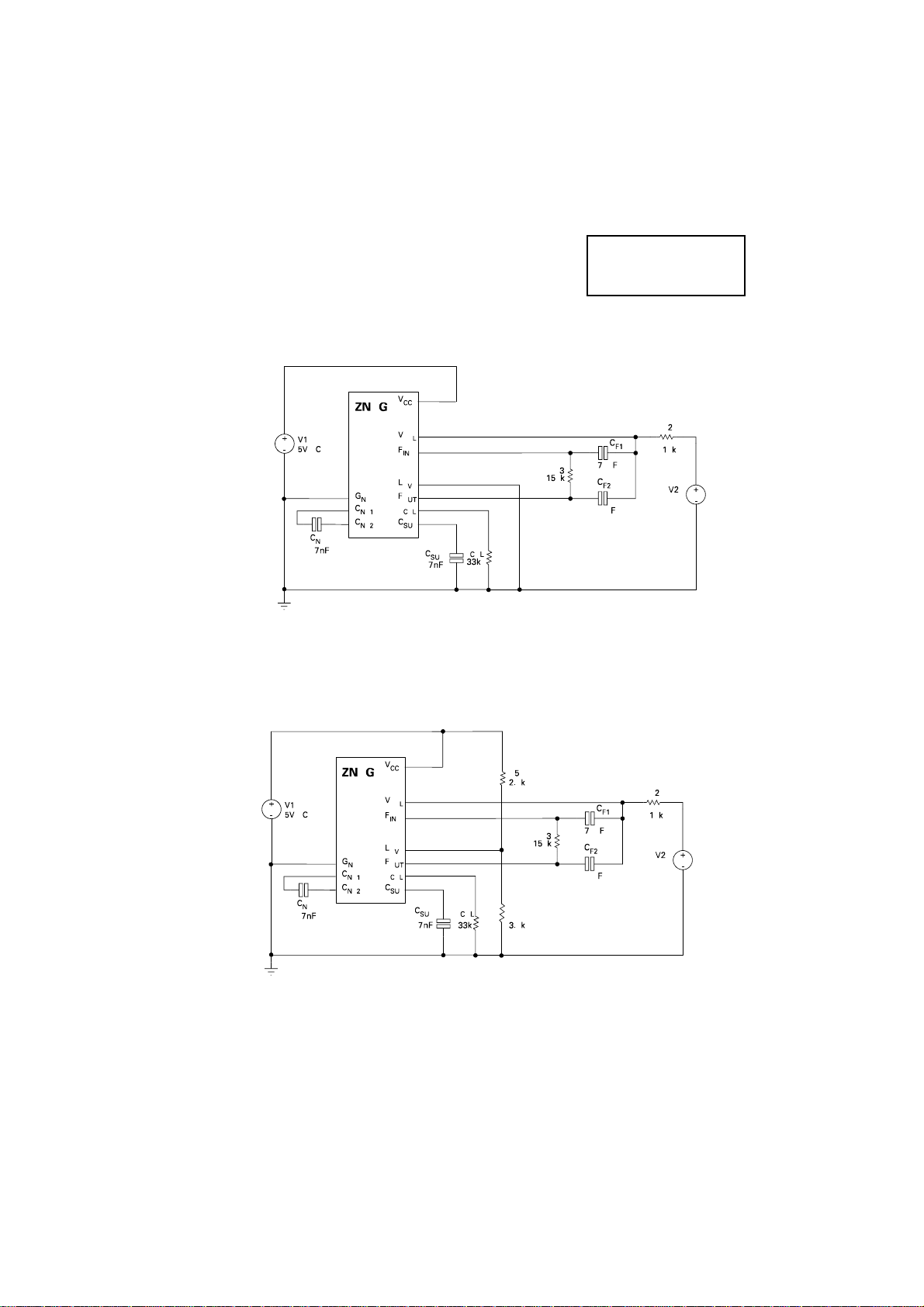
TONE DETECTION CHARACTERISTICS
Filter Amplifier
I
B
V
I
OUT
G
V
I
LEAK
Input Bias Current
Output Voltage
OUT
Output Current 5V
Voltage Gain f=22kHz,VIN=1mV 46 dB
V
Rectifier
Output Voltage
OUT
Leakage Current
=150kΩ
R
F1
5
RF1=150kΩ
=1.96V, V
OUT
5
RF1=150kΩ IL=-10µA
5
RF1=150kΩ V
=2.1V 400 520 650
FIN
=3V
OUT
0.04 0.15 1.0
1.75 1.95 2.05 V
1.8 2.0 2.2
20 200 nA
Comparator
TH
Threshold
Voltage
5
f=0 2.95 3.2 3.45 V
V
Output Stage
V
I
V
V
V
V
LOV
LOV
LBL
LBH
HBL
HBH
Volt. Range IL=50mA(LB or HB)-0.5V
L
OV
LOV Bias Current V
LB Output Low
LB Output High V
HB Output Low
HB Output High V
=0 0.04 0.15 1.0
LOV
=0 IL=-10µA Enabled
V
LOV
V
=3V IL=0 Enabled
LOV
=0 IL=10mA Disabled
LOV
V
=3V IL=50mA Disabled
LOV
=0 IL=-10µA Enabled
V
LOV
V
=3V IL=0 Enabled
LOV
=0 IL=10mA Disabled
LOV
V
=3V IL=50mA Disabled
LOV
6
7
6
7
6
7
6
7
-3.5
-0.01
-0.025
2.903.0
-3.5
-0.01
-0.025
2.903.0
-2.750-2.5
-2.750-2.5
CC
0.01VV
0.025
3.1VV
0.01VV
0.025
3.1VV
POLARITY SWITCH CHARACTERISTICS
I
POL
V
T
NOTES:
1. The negative bias voltages specified are generated on-chip using an internal oscillator. Two external capacitors, C
47nF are required for this purpose.
2. The characteristics are measured using an external reference resistor R
3. Noise voltage is not measured in production.
4. Noise voltage measurement is made with FETs and gate and drain capacitors in place on all o utputs. C
gate outputs and ground, C
5 . These parameters are lneearly related to V
6. These parameters are measured using Test Circuit 1
7. These parameters are measured using Test Circuit 2
TPOL
SPOL
Input Current
Threshold
Voltage
Switching Speed
, 10nF, are connected between drain outputs and ground.
D
=25V (Applied via R
V
POL
=25V (Applied via R
V
POL
=25V (Applied via R
V
POL
CC
=10kΩ)
POL
=10kΩ)
POL
=10kΩ)
POL
of value 33k wired from pins R
CAL
10 20 40
14 14.75 15.5 V
100 ms
to ground.
CAL
, 4.7nF, are connected between
G
-1.8 V
and C
NB
UNITS
µA
µA
V
µA
µA
SUB
, of
4-126
TEST CIRCUIT 1
TEST CIRCUIT 2
ZNBG3113
ZNBG3114
V2 Characteristics
Type AC source
Frequency 22kHz
Voltage 350mV p/p enabled
100mV p/p disabled
V2 Characteristics
Type AC source
Frequency 22kHz
Voltage 350mV p/p enabled
100mV p/p disabled
4-127
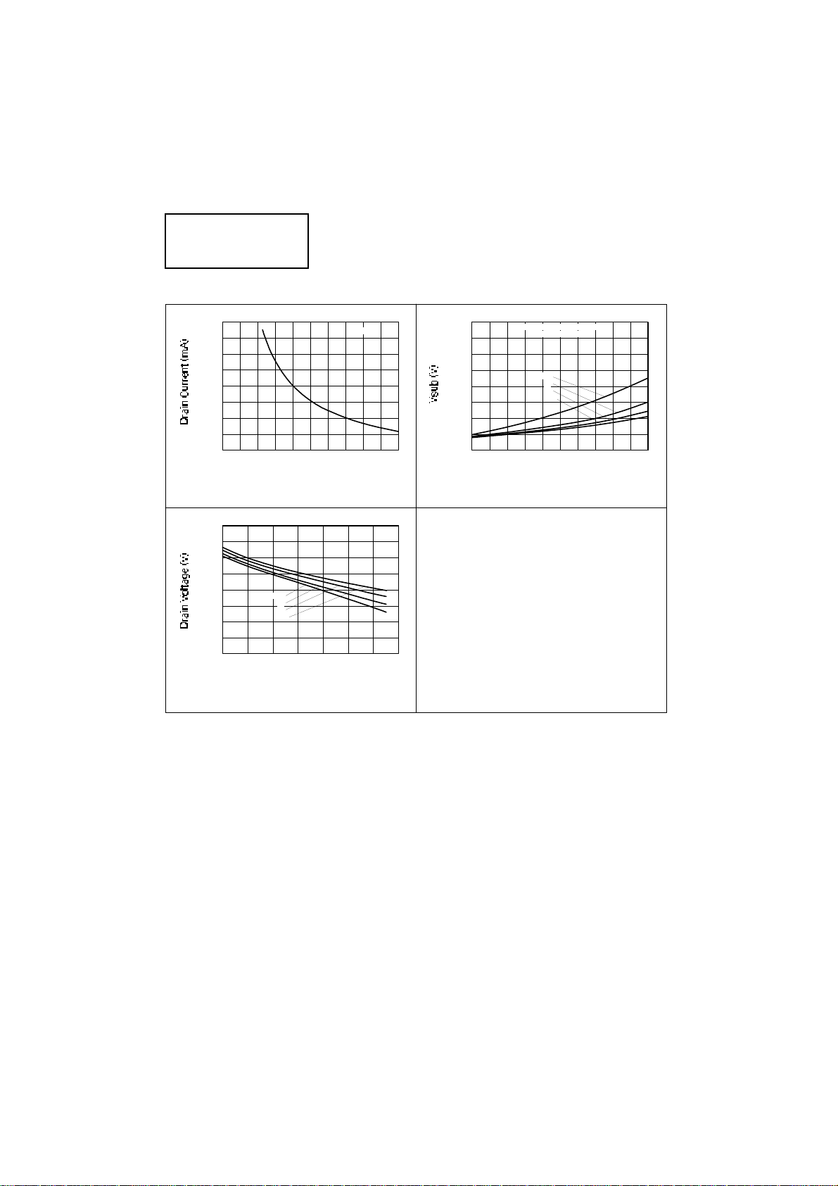
ZNBG3113
ZNBG3114
TYPICAL CHARACTERISTICS
16
14
12
10
8
6
4
2
0
0204060 100
R
(k)
cal
Vcc = 5V
80
JFET Drain Current v Rcal
2.4
2.3
2.2
2.1
2.0
Vcc = 5V
6V
8V
10V
2468 16
10
12 14
Drain Current (mA)
JFET Drain Voltage v Drain Current
Note:- Operation with loads > 2 00µA
0.0
-0.5
-1.0
-1.5
-2.0
-2.5
-3.0
0 0.2 0.4 0 .6 1.0
is not guaranteed.
Vcc = 5V
6V
8V
10V
External Vsub Load (mA)
Vsub v External Load
0.8
4-128
 Loading...