

Page 1
ZMT32
()
()
α
α
α
2
2
2
1
2
Tan
Cos
Sin
V
V
O
O
==
-VO1(cos)
-V
O2
(sin)
V
CC2
(bridge 2)
V
CC1
(bridge 1)
+V
O1
(cos)
+V
O2
(sin)
GND2 (bridge 2)
GND (bridge 1)
2
3
4
5
6
7
8
1
Magnetic Field Angle Sensor
Description
The ZMT32 is a thin film permalloy magnetic
field sensor, which contains two galvanic
isolated Wheatstone Bridges for high
precision angle measurement applications
under low field conditions. This angle sensor
is based on the anisotropic magnetoresistive
effect (AMR). The two internal (V
CC1
, V
CC2
bridges enclose a relative sensitive angle of
45 degrees. The input field is a rotating
magnetic field in the chip plane (parallel to
the surface of package). This rotating field will
make available two independent sinusoidal
output signals with the following relationship
()
where α = angle between sensor axis and field
direction
The precise ZMT32 works with low field
applications (H
than similar devices. The ultimate output signal
quality depends on the external magnetic
material and on the mechanical realization.
)
The ZMT32 is a passive part and the ArcTangent interpolation needs external signal
processing. Typical areas of application are
angle and speed measurement.
= 8 to 25kA/m), much lower
rot
Features
• contactless angle measurement up to 180°
• flexible measuring solutions for moved
systems
• stable operation over long time
• high temperature range up to +160°C
Applications
• angle and angular velocity measuring systems
• absolute angle and angle change
• automotive electronic (steering, throttle
control, pedal positioning, etc
• contactless rotary switches and potentiometer
• automatic adjustment
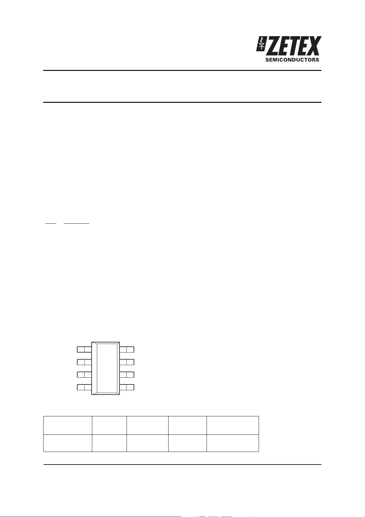
Ordering Information
Device Reel size
(Inches)
ZMT32TA 7 12 1,000 ZETEX
Tape w idt h
(mm)
Quantity
per reel
Device
marking
ZMT32
Issue 1 - June 2008 1 www.zetex.com
© Zetex Semiconductors plc 2008
Page 2
ZMT32
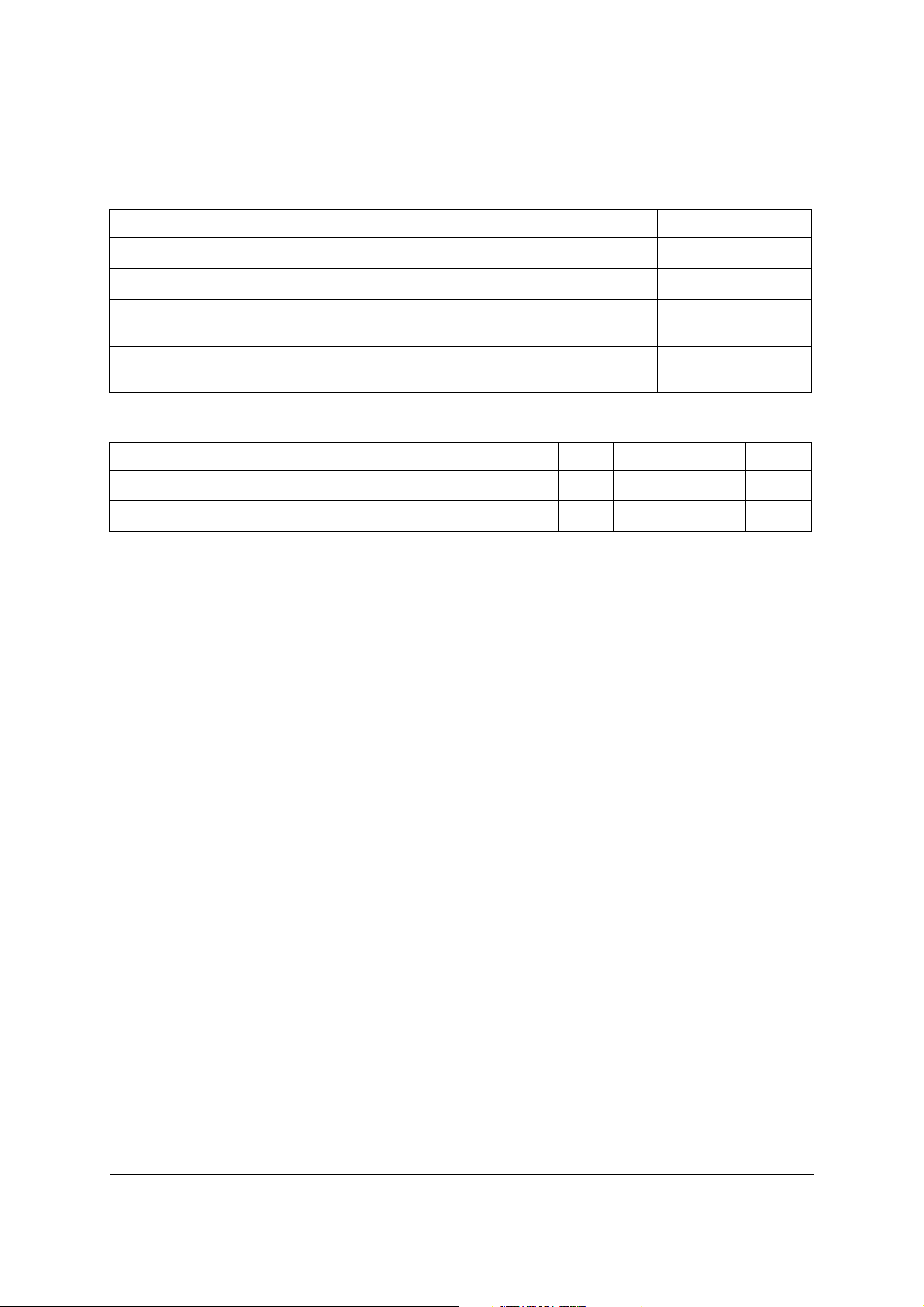
Absolute maximum ratings
Parameter Symbol Limit Unit
Supply Voltages V
Single Bridge Current I
Operating Temperature
T
cc1
cc1
A
and V
or I
cc2
cc2
10 V
4 mA
-40 to +160 °C
Range
Storage Temperature
T
-55 to +175 °C
stg
Range
Recommended operating conditions
Symbol Parameter Min Typ Max Unit
V
, V
cc1
cc2
H
rot
Supply Voltages 5 8.5 V
Applied Magnetic Field Strength 8 25 kA/m
Issue 1 - June 2008 2 www.zetex.com
© Zetex Semiconductors plc 2008
Page 3
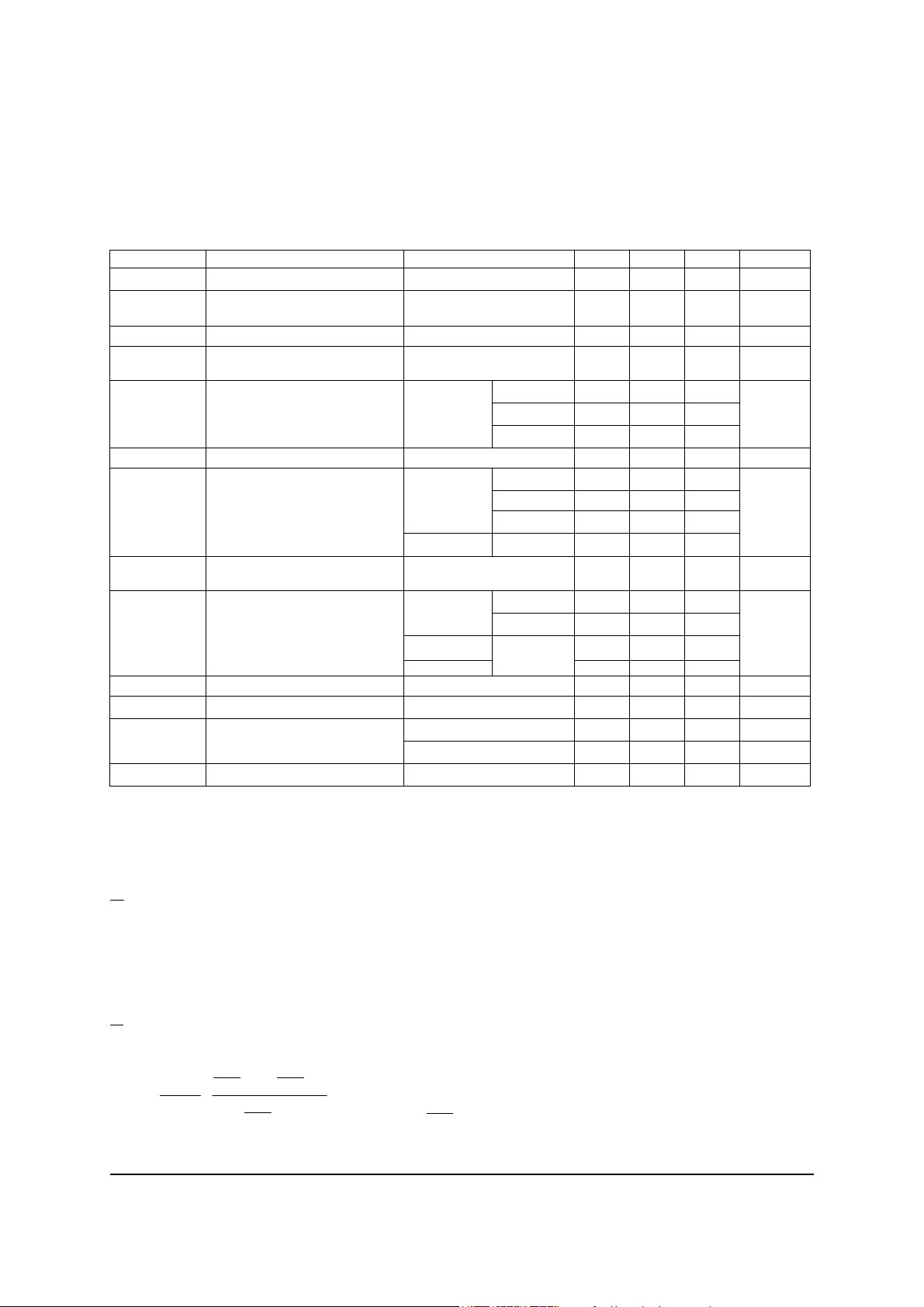
Electrical characteristics
NOTES:
%100
)T(
V
V
)T(
V
V
)T(
V
V
TT
1
TCV
0
CC
O
1
CC
O
2
CC
O
12
O
×
Δ
Δ
−
Δ
×
−
=
)T(
V
V
n
CC
O
Δ
General test conditions (unless otherwise noted)
TA= +23±5oC, V
CC1=VCC2
= +5V, H
ROT
=25kA/m
SYMBOL PARAMETER CONDITIONS MIN
Sα1 or S
V
PO1
or V
Sensitivities (zero crossing)
α2
Peak Output Voltages
PO2
(sinusoidal signals)
k Amplitude bridge matching 99.77 100 100.23 %
Temperature coefficient of
amplitude bridge matching
Bridge resistances
B
TC of Bridge Resistances +0.28 +0.32 +0.36 %/K
B
A
Peak to peak output swing
A
TC of peak to peak output
B
O
swing
A
CC1
Output offset voltage
A
CC2
B
TC of output offset voltage -4 0 +4 µV/V/K
A
Angular Inaccuracy 0.05 0.2 deg
A
Angular hysteresis
Isolation Bridge Current
TCR
∆V
O1/VCC1
∆V
O2/VCC2
TCV
V
OFF1
V
OFF2
TCV
TCk
R
B1
or
R
B2
or
or
∆α
∆αH
I
iso1-2
/V
/V
OFF
(†)
, k=100•(V
α1=135°, α2=0°
TA = -40 to +160°C
no H
ROT
H
= 8 kA/m
ROT
H
= 8 kA/m
ROT
no H
ROT
H
ROT
no H
PO1/VPO2
TA = -40°C
TA = 23°C
TA = +160°C
TA = -40°C
TA = 23°C
TA = +160°C
(†)
T
TA = -40°C
TA = +160°C
(†)
T
= 8 kA/m
ROT
= 23°C
A
= 23°C
A
(†)
) with V
CC1=VCC2
TYP
(*)
0.35 mV/V/deg
40 50 60 mV
-0.008 +0.008 %/K
2017 3040
2500 3000 3600
3345 5114
19.2 30.4
16 20 24
6.7 13.4
16 20 24
-0.35 -0.32 -0.28 %/K
-1.25 +1.25
-1.55 +1.55
-1 0 +1
-2 0 +2
00.1µA
ZMT32
MAX UNIT
Ω
mV/V
mV/V
0.1 deg
0.5
(‡)
deg
(*) Typical values apply to an ambient temperature of 23oC
(†) See point “Magnetic Field Tests” below
(‡) The accurate control of this parameter (Lim
=0.1deg, H
max
=25kA/m) takes place by means of sample tests
ROT
A: Output characteristic definitions
∆VO1/V
V
OFF1/VCC1
∆αH = MAX | α
∆α = MAX | α
CC1
= (V
= ½(V
o
– V
OMAX1
OMAX1
LEFT TURN
OMIN1
+ V
OMIN1
– α
RIGHT TURN
)/V
or/ ∆VO2/V
CC1
)/V
or/ V
CC1
= (V
CC2
OFF2/VCC2
OMAX2
= ½(V
– V
OMAX2
OMIN2
+ V
)/V
CC2
OMIN2
)/V
| (max. angular difference between left and right turn)
CC2
– α | (max. angular difference between actual value αoand measured angle,
without offset error)
B: Temperature coefficient (TC) equations
T1 = -25°C, T0 = +25°C, T2 = +125°C
where
is the peak-peak output voltage at temperature T
n
Issue 1 - June 2008 3 www.zetex.com
© Zetex Semiconductors plc 2008
Page 4

ZMT32
%100
)T(R
)T(R)T(R
TT
1
TCR
0B
1B2B
12
B
×
−
×
−
=
)TT(
VV
TCV
12
)1T(OFF)2T(OFF
OFF
−
−
=
⎟
⎟
⎠
⎞
⎜
⎜
⎝
⎛
=α=
1O
2O
V
V
arctan]anglemeasured[
where R
where V
) is the bridge resistance at temperature T
B(Tn
is the output offset voltage at temperature T
OFF(Tn)
n
n
Magnetic field tests
For these tests a rotating magnetic field is generated and the output signals of both bridges are measured at
four different field angles for right rotation as well as for left rotation. Using these measured output signals
the diameter and the center coordinates of the best circle are calculated. They correspond to the output
voltage range and the offset voltage. Furthermore the field angles for both rotation directions and angular
hysteresis are calculated
Method
The data pairs are transformed onto a unit circle starting from their position in the data collection
for determining direction information or angle information.
It must be evaluated with four pair values (cos, sin) on a right rotation (magnetic field rotation)
and four pair values (cos, sin) on a left rotation (magnetic field rotation).
The field rotation steps are:
Æ start in 180° position
§ right rotation to 22.5° with measurement of sensor outputs
§ right rotation to 67.5° with measurement of sensor outputs
§ right rotation to 112.5° with measurement of sensor outputs
§ right rotation to 157.5° with measurement of sensor outputs
§ right rotation to 0° (360°) , stop , reversal
§ left rotation to 157.5° with measurement of sensor outputs
§ left rotation to 112.5° with measurement of sensor outputs
§ left rotation to 67.5° with measurement of sensor outputs
§ left rotation to 22.5° with measurement of sensor outputs , end position
General description of tests with external magnetic field.
Issue 1 - June 2008 4 www.zetex.com
© Zetex Semiconductors plc 2008
Page 5

Operating principle
e
e
-V
O1
-V
O2
V
cc1
V
cc2
GND1
GND2
+V
O1
+V
O2
1
-15
-10
-5
0
5
10
0 45 90 135 180 225 270 315 360
Output vol tage (mV /V )
Cos 2
α
Sin 2
α
Sensor bridge 2
Sensor bridge 1
ZMT32
GND1
H
O
rot
0
8
Bridg
1
␣
α = 0°
1
1
-
O1
V
GND2
7
2
-V
O2
+V
6
Bridg
2
3
V
CC2
O2
O1
+V
5
4
V
CC1
When a common-magnetic field is applied through the
ZMT32 the 2 internal magneto-resistive bridges are
affected slightly differently due to their 45° rotation to
one another. This 45° rotation enables the ZMT32 to
determine angular position, of a rotating magnetic
field.
When a rotating magnetic field is applied to the ZMT32
it will output 2 sinusoidal voltages that are:
• proportional to the field strength applied
• proportional to the supply voltage applied,
• rotating at twice the angular position
Characteristic output curves V
O1
, V
O2
Issue 1 - June 2008 5 www.zetex.com
© Zetex Semiconductors plc 2008
• 90° apart (as seen below).
By taking the arcTan of the ratio of V
to VO1 the
O2
angular position of the magnetic field can be
determined.
Page 6

Typical characteristics
0.0%
0.2%
0.4%
0.6%
0.8%
1.0%
1.2%
1.4%
01020304050
H
ROT
- Field strength (kA/m)
Angle accuracy
0
5
10
15
20
25
01020304050
Accuracy variance with field strength
V
CC1=VCC2
=+5V
T
A
=23oC
k=100
Output variance with magnetic field strength
H
ROT
- Field strength (kA/m)
Output voltage (mV/V)
V
CC1=VCC2
=+5V
T
A
=23oC
k=100
ZMT32
Issue 1 - June 2008 6 www.zetex.com
© Zetex Semiconductors plc 2008
Page 7

Typical characteristics
0
5
10
15
20
25
30
35
-50 -25 0 25 50 75 100 125 150 175
MAX
MIN
0
1000
2000
3000
4000
5000
6000
-50 -25 0 25 50 75 100 125 150 175
MAX
MIN
Output voltage versus temperature
Temperature (
o
C)
Output voltage (mV/V)
V
CC1=VCC2
=+5V
T
A
=23oC
k=100
V
CC1=VCC2
=+5V
T
A
=23oC
k=100
Temperature (oC)
Bridge resistance (Ω)
Bridge resistance versus temperature
ZMT32
Issue 1 - June 2008 7 www.zetex.com
© Zetex Semiconductors plc 2008
Page 8

Typical application
CC
+V
result of angle
measurement
ZMT32
GND
OUT1
V
-
tan
D
A
p
D
A
OUT2
V
fixed 45 degree phase
difference between
outputs 1 and 2
-
+
+
R2
41
COS
R1
top view
ZMT32T8
R1
SIN
85
R3
R4
R3
R2
R4
Issue 1 - June 2008 8 www.zetex.com
© Zetex Semiconductors plc 2008
Page 9

ZMT32
2.8
0.110
6.8
0.268
4.6
0.181
0.95
0.037
1.52
0.060
mm
inches
Package outline - SM-8 Soldering footprint
DIM Millimeters Inches DIM Millimeters Inches
Min. Max. Typ. Min. Max. Typ. Min. Max. Typ. Min. Max. Typ.
A - 1.7 - - 0.067 - e1 - - 4.59 - - 0.1807
A1 0.02 0.1 - 0.0008 0.004 - e2 - - 1.53 - - 0.0602
b - - 0.7 - - 0.0275 He 6.7 7.3 - 0.264 0.287 -
c 0.24 0.32 - 0.009 0.013 - Lp 0.9 - - 0.035 - -
D 6.3 6.7 - 0.248 0.264 - ␣ - 15° - - 15° -
E 3.3 3.7 - 0.130 0.145 -  - - 10° - - 10°
Note: Controlling dimensions are in millimeters. Approximate dimensions are provided in inches
Issue 1 - June 2008 9 www.zetex.com
© Zetex Semiconductors plc 2008
Page 10

ZMT32
Definitions
Product change
Zetex Semiconductors reserves the right to alter, without notice, specifications, design, price or conditions of supply of any product or
service. Customers are solely responsible for obtaining the latest relevant information before placing orders.
Applications disclaimer
The circuits in this design/application note are offered as design ideas. It is the responsibility of the user to ensure that the circuit is fit for
the user’s application and meets with the user’s requirements. No representation or warranty is given and no liability whatsoever is
assumed by Zetex with respect to the accuracy or use of such information, or infringement of patents or other intellectual property rights
arising from such use or otherwise. Zetex does not assume any legal responsibility or will not be held legally liable (whether in contract,
tort (including negligence), breach of statutory duty, restriction or otherwise) for any damages, loss of profit, business, contract,
opportunity or consequential loss in the use of these circuit applications, under any circumstances.
Life support
Zetex products are specifically not authorized for use as critical components in life support devices or systems without the express written
approval of the Chief Executive Officer of Zetex Semiconductors plc. As used herein:
A. Life support devices or systems are devices or systems which:
1. are intended to implant into the body
or
2. support or sustain life and whose failure to perform when properly used in accordance with instructions for use provided in the
labelling can be reasonably expected to result in significant injury to the user.
B. A critical component is any component in a life support device or system whose failure to perform can be reasonably expected to
cause the failure of the life support device or to affect its safety or effectiveness.
Reproduction
The product specifications contained in this publication are issued to provide outline information only which (unless agreed by the
company in writing) may not be used, applied or reproduced for any purpose or form part of any order or contract or be regarded as a
representation relating to the products or services concerned.
Terms and Conditions
All products are sold subjects to Zetex’ terms and conditions of sale, and this disclaimer (save in the event of a conflict between the two
when the terms of the contract shall prevail) according to region, supplied at the time of order acknowledgement.
For the latest information on technology, delivery terms and conditions and prices, please contact your nearest Zetex sales office.
Quality of product
Zetex is an ISO 9001 and TS16949 certified semiconductor manufacturer.
To ensure quality of service and products we strongly advise the purchase of parts directly from Zetex Semiconductors or one of our
regionally authorized distributors. For a complete listing of authorized distributors please visit: www.zetex.com/salesnetwork
Zetex Semiconductors does not warrant or accept any liability whatsoever in respect of any parts purchased through unauthorized sales channels.
ESD (Electrostatic discharge)
Semiconductor devices are susceptible to damage by ESD. Suitable precautions should be taken when handling and transporting devices.
The possible damage to devices depends on the circumstances of the handling and transporting, and the nature of the device. The extent
of damage can vary from immediate functional or parametric malfunction to degradation of function or performance in use over time.
Devices suspected of being affected should be replaced.
Green compliance
Zetex Semiconductors is committed to environmental excellence in all aspects of its operations which includes meeting or exceeding
regulatory requirements with respect to the use of hazardous substances. Numerous successful programs have been implemented to
reduce the use of hazardous substances and/or emissions.
All Zetex components are compliant with the RoHS directive, and through this it is supporting its customers in their compliance with
WEEE and ELV directives.
Product status key:
“Preview” Future device intended for production at some point. Samples may be available
“Active” Product status recommended for new designs
“Last time buy (LTB)” Device will be discontinued and last time buy period and delivery is in effect
“Not recommended for new designs”
“Obsolete” Production has been discontinued
Datasheet status key:
“Draft version” This term denotes a very early datasheet version and contains highly provisional information, which
“Provisional version” This term denotes a pre-release datasheet. It provides a clear indication of anticipated performance.
“Issue” This term denotes an issued datasheet containing finalized specifications. However, changes to
Zetex sales offices
Europe
Zetex GmbH
Kustermann-Park
Balanstraße 59
D-81541 München
Germany
Telefon: (49) 89 45 49 49 0
Fax: (49) 89 45 49 49 49
europe.sales@zetex.com
© 2008 Published by Zetex Semiconductors plc
Device is still in production to support existing designs and production
may change in any manner without notice.
However, changes to the test conditions and specifications may occur, at any time and without notice.
specifications may occur, at any time and without notice.
Americas
Zetex Inc
700 Veterans Memorial Highway
Hauppauge, NY 11788
USA
Telephone: (1) 631 360 2222
Fax: (1) 631 360 8222
usa.sales@zetex.com
Asia Pacific
Zetex (Asia Ltd)
3701-04 Metroplaza Tower 1
Hing Fong Road, Kwai Fong
Hong Kong
Telephone: (852) 26100 611
Fax: (852) 24250 494
asia.sales@zetex.com
Corporate Headquarters
Zetex Semiconductors plc
Zetex Technology Park, Chadderton
Oldham, OL9 9LL
United Kingdom
Telephone: (44) 161 622 4444
Fax: (44) 161 622 4446
hq@zetex.com
Issue 1 - June 2008 10 www.zetex.com
© Zetex Semiconductors plc 2008
 Loading...