

Page 1
Issue 4 - July 2006
© Zetex Semiconductors plc 2006
SUPPLY VOLTAGE
MONITOR
ISSUE 4 – JULY 2006
ZM33164-3
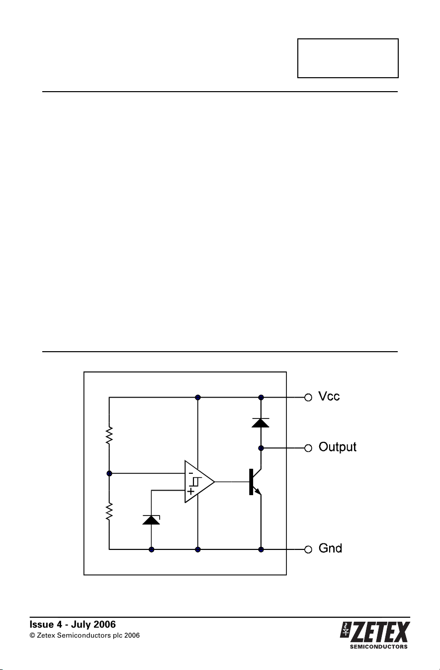
DEVICE DESCRIPTION
The ZM33164-3 is a three terminal under
voltage monitor circuit for use in
microprocessor systems. The threshold
voltage of the device has been set to 2.68
volts making it ideal for 3 volt circuits.
Included in the device is a precise voltage
reference and a comparator with built in
hysteresis to prevent erratic operation. The
ZM33164-3 features an ope n collector output
capable of sinking at least l0mA which only
requires a single external resistor to
interface to following circuits.
Operation of the device is guaranteed from
one volt upwards, from this level to the
device threshold voltage the output is held
low providing a power on reset function.
Should the supply voltage, once established,
at any time drop below the threshold level
then the output again will pull low.
The device is available in a TO92 package for
through hole applications as well as SOT223
for surface mount requirements.
SCHEMATIC DIAGRAM
FEATURES
SOT223 and TO92 packages
•
Power on reset generator
•
Automatic reset generation
•
Low standby current
•
Guaranteed operation from 1 volt
•
Wide supply voltage range
•
Internal clamp diode to discharge delay
•
capacitor
2.68 volt threshold for 3 volt logic
•
60mV hysteresis prevents erratic operation
•
APPLICATIONS
Microprocessor systems
•
Computers
•
Computer peripherals
•
Instrumentation
•
Automotive
•
Battery powered equipment
•
4-99
Page 2
Issue 4 - July 2006 www.zetex.com
© Zetex Semiconductors plc 2006
ZM33164-3
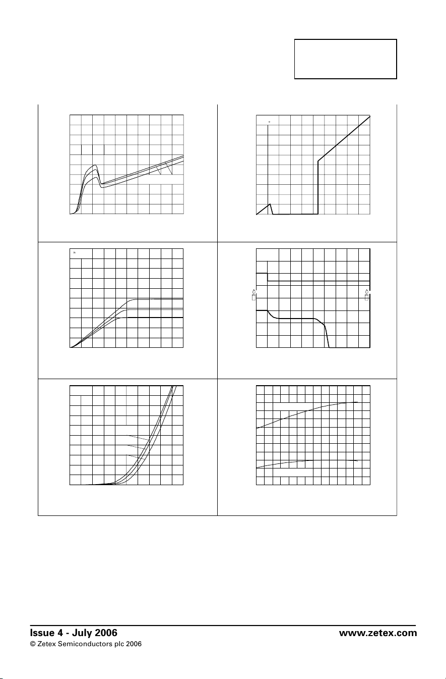
TYPICAL CHARACTERISTICS
500
400
A)
µ
300
5
RL =10K
T
A=25
°C
4
3
200
Input Current (
100
0
0246810
-40 °C 25 °C 85 °C
Input Voltage (V)
Output Voltage (V)
2
1
0
01
2 345
Input Voltage (V)
Input Current vs. Input Voltage Output Voltage vs. Input Voltage
50
Vin=2.4V
40
30
20
Sink Current (mA)
10
0
00.8 1.62.00.4 1.2
Output Saturation Voltage (V)
-40 °C
25 ° C
85 ° C
R
L=10K
3.0
2.4
Vin
(V)
4
2
Vout
(V)
0
012
Tim e (µs)
3
Output Saturation Voltage vs. Sink Current Reset Delay Time
100
V
0V
=
in
80
60
40
Forward Current ( mA)
20
0
00.4 2.00.8 1.2 1.6
85 ° C
25 °C
-40 °C
2.77
2.75
2.73
2.71
2.69
Threshold Voltage (V)
2.67
2.65
Upper Threshold
Lower Threshold
-40
-20 0 20 40 60 80
Temperature ( °C)Forward Voltage (V)
Clamp Diode Forward Current vs. Voltage Threshold Voltage vs. Temperature
4
100
4-101
Page 3

Issue 4 - July 2006 www.zetex.com
© Zetex Semiconductors plc 2006
ZM33164-3
ABSOLUTE MAXIMUM RATING
Input Supply Voltage -1 to 12V
Offstate Output Voltage 12V
Onstate Output
Sink Current(
Clamp diode
Forward Current(
Operating junction
temperature 150°C
Operating Temperature -40 to 85°C
Storage Temperature -65 to 150°C
TEST CONDITIONS
(T
amb
COMPARATOR
PARAMETER SYMBOL
Threshold Voltage
High state output (Vcc increasing) V
Threshold Voltage
Low state output (Vcc decreasing) V
Hysteresis V
OUTPUT
Output sink saturation: V
(Vcc=2.4V, I
(V
cc
(V
cc
Onstate output sink current
(V
, Output=2.4V)
cc
Offstate output leakage current
, Output=3V)
(V
cc
Clamp diode forward voltage
=10mA)
(I
f
Propagation delay
3V to 2.4V, Rl=10k, T
(V
in
TOTAL DEVICE
Operating input voltage range V
Quiescent input current (V
Note 1) Internally limited
Note 1)100mA
=25°C for typical values, T
=8.0mA) 0.46 1.0 V
sink
=2.4V, I
=1.0V, I
=2.0mA) 0.15 0.4 V
sink
=0.1mA) 0.25 V
sink
=25°C)
amb
=3V) I
cc
=-40 to 85°C for min/max values (Note3))
amb
IH
IL
H
OL
I
sink
I
oh
V
f
T
d
cc
q
Power Dissipation
TO92 780mW
SOT223 2W(
MIN TYP. MAX.
Note 2)
UNITS
2.55 2.71 2.8 V
2.55 2.65 2.8 V
0.03 0.06 0.15 V
10 20 60 mA
0.02 0.5
µA
0.61.21.5V
2.5
µs
1.0 to 10 V
125 190
µA
4-100
Page 4

Issue 4 - July 2006 www.zetex.com
© Zetex Semiconductors plc 2006
ZM33164-3
TIMING DIAGRAM
Vcc
Threshold
Vol t ag e
1V
Output
Output
Undefined
APPLICATION CIRCUIT
Note 4: A time delayed reset can be accomplished with the additional Cd.
1
TDY = RCd ln
æ
ç
ç
1
−
ç
è
V
TH(mpu )
V
ö
÷
÷
÷
in
ø
TDY =Time (Seconds)
=Microprocessor Reset Threshold
V
TH
V
=Power Supply Voltage
in
Output
Undefined
4-102
Page 5

For international sales offices visit www.zetex.com/offices
Zetex products are distributed worldwide. For details, see www.zetex.com/salesnetwork
This publication is issued to provide outline information only which (unless agreed by the company in writing) may not be
used, applied or reproduced for any purpose or form part of any order or contact or be regarded as a representation relating
to the products or services concerned. The company reserves the right to alter without notice the specification, design, price
or conditions of supply of any product or service.
Europe
Zetex GmbH
Streitfeldstraße 19
D-81673 München
Germany
Telefon: (49) 89 45 49 49 0
Fax: (49) 89 45 49 49 49
europe.sales@zetex.com
Americas
Zetex Inc
700 Veterans Memorial Highway
Hauppauge, NY 11788
USA
Telephone: (1) 631 360 2222
Fax: (1) 631 360 8222
usa.sales@zetex.com
Asia Pacific
Zetex (Asia Ltd)
3701-04 Metroplaza Tower 1
Hing Fong Road, Kwai Fong
Hong Kong
Telephone: (852) 26100 611
Fax: (852) 24250 494
asia.sales@zetex.com
Corporate Headquarters
Zetex Semiconductors plc
Zetex Technology Park, Chadderton
Oldham, OL9 9LL
United Kingdom
Telephone: (44) 161 622 4444
Fax: (44) 161 622 4446
hq@zetex.com
Issue 4 - July 2006 www.zetex.com
© Zetex Semiconductors plc 2006
CONNECTION DIAGRAMS
ZM33164-3
TO92 Package Suffix – C
Bottom View
ORDERING INFORMATION
Part Number Package Part Mark
ZM331643G SOT223 ZM331643
ZM331643C TO92 ZM331643
SOT223 Package Suffix – G
Top View –
Pin 4 floating or connected to pin 2
4-103
 Loading...