

Page 1

A
f
ZLNB254
Dual DiSEqC™ Interface IC
SUMMARY
The ZLNB254 is a dual channel DiSEqC™ interface for S atellite Low Noise Blocks
(LNB’s) and distribution systems. Providing two accurate DiSEqC™ detectors the
ZLNB254 converts the DiSEqC™ signals into logic level representations enabling
reliable and easy detection for a microprocessor. Packaged in a small footprint
DFN and only requiring two external components per channel th e complete solution
is cost effective and requires minimal PCB space.
FEATURES
• Dual Channel DiSEqC™ interface
• Reliable and accurate detectors
• High channel isolation
• Compatible with Eutelsat and US specifications
• Simple and easy to design in.
• Outputs compatible with LSTTL and CMOS loads
• Operates over a wide supply voltage
• Temperature compensated
APPLICATIONS
• DiSEqC™ controlled LNB’s
• Satellite distribution systems
• Mono Block LNB’s
• DiSEqC Actuators
• Set-Top Boxes
• Satellite Test Equipment
• AC satellite control signal detection
Product Line o
Diodes Incorporated
2
2
5
5
4
4
ZLNB254
Document number: Ds32002 Rev. 1
1 of 8
www.diodes.com
October 2009
© Diodes Incorporated
Page 2
DESCRIPTION
The ZLNB254 is a dual DiSEqC™ tone detector IC for
multiple output LNBs, satellite distribution systems,
set-top boxes and DiSEqC™ peripherals. Although
intended for use with 22kHz DiSEqC™ signals, the
ZLNB254 can be used over the frequency range of
10kHz to 60kHz so it can detect standard 22kHz
satellite band control signals as well as regional
variations such as those in Japan.
The minimum of external components are required to
enable this two-channel tone filter and fast envelope
detector. The ZLNB254 is particularly suited to low
signal level, high distortion DiSEqC™ signal detecting
applications.
The ZLNB254 includes circuitry necessary to detect
the presence of a 22kHz tones modulated on the
supply inputs to a LNB or switchbox. The TD outputs
are set low on detection of a valid tone or DiSEqC™
signal when applied to the FIN inputs.
To enable system flexibility user control is given over
the gain and the lower frequency limit of the filter by
using a single external resistor and capacitor per
channel. The higher frequency limit of the filters is set
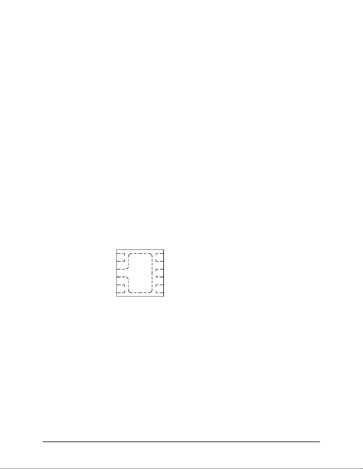
Pinout Diagram
TDFN2020-6 Top view
1
TD2
2
GND
3
FIN1
6
TD1
5
VCC
4
FIN2
ZLNB254
internally above 60kHz. The remaining detector
circuits utilises no other external components.
The tone detector can be used to sense either
continuous tones or coded tone bursts such as used
in DiSEqC™ and similar control systems. To ensure
system reliability the tone detector rejects unwanted
signals including transients from other parts of the
LNB system without the use of any external
components.
The TD outputs are designed to be compatible with
LSTTL and CMOS loads so can drive a
microcontroller or other logic directly.
To give further protection the resistor which is used to
set the filter gain also provides ESD protection.
The ZNBL254 provides a small simple solution and is
packaged in the TDFN2020-6 surface mount
package.
ZLNB254
Document number: Ds32002 Rev. 1
2 of 8
www.diodes.com
October 2009
© Diodes Incorporated
Page 3
(1)
ZLNB254
Absolute Maximum Ratings
Supply Voltage -0.6V to +15V
Supply Current 50mA
Power Dissipation 350mW
Operating Temperature Range -40°C to +85°C
Storage Temperature Range -40°C to +125°C
Electrical Characteristics
Measured at Tamb = 25°C, Vcc = 5V unless otherwise specified.
Parameter Conditions Limits
Min Typ Max
Supply Voltage
Operating Range
Supply Current All outputs unloaded, any combination of valid
Tone Detectors
AC Thresh
Switching Delay TD outputs, Test Circuit 2 100 150 us
TD Outputs
Voltage High ITD = -2mA, Test Circuit 1, Tone disabled Vcc-0.5 Vcc-0.2 Vcc V
Voltage Low ITD = 5mA, Test Circuit 1, Tone enabled 0 0.29 0.5 V
Notes: 1. The tone detector threshold is Vcc dependent. See Application section for details.
Test Circuit 1 100 140 200 mVp/p
inputs.
3.0 8 V
0.7 2 mA
Units
ZLNB254
Document number: Ds32002 Rev. 1
3 of 8
www.diodes.com
October 2009
© Diodes Incorporated
Page 4

Test Circuit 1
Test Circuit 2
TD2
GND
FIN1
ZLNB254
ZLNB254
1
2
3
Note 1: V2 Characteristics
TD1
6
VCC
5
FIN2
4
Ty pe:- AC source
Frequency:- 22kHz
Wav eform:- Squarewave, 7.5us tr/tf
100pF
C1
V1
5V
R1
62k
V2
(See Not e 1)
TD2
1
GND
2
FIN1
3
Note 1: V2 Characteristics
Type:- AC source
Frequency:- 22kHz
Voltage: - 300m Vp/ p Enabled
ZLNB254
Zero D is abled
V1
5V
TD1
6
VCC
5
FIN2
4
100pF
C1
R1
62k
V2
(See Not e 1)
Tone Input (V2)
TD Output
ZLNB254
Document number: Ds32002 Rev. 1
Switching Delays
4 of 8
www.diodes.com
October 2009
© Diodes Incorporated
Page 5

Typical Characteristics
ZLNB254
Icc vs. Vcc vs. Input state
Icc vs. Vcc vs. Temperature
ZLNB254
Document number: Ds32002 Rev. 1
5 of 8
www.diodes.com
October 2009
© Diodes Incorporated
Page 6

APPLICATIONS INFORMATION
ZLNB254
Vcc
ZLNB254
Micro-Controller
Vcc
P1
P2
P3
P4
Gnd
ZLN B254 Applicat ion Circ uit
@ Zetex plc 2009
TD2
GND
FIN1
1
2
3
TD1
6
VCC
5
FIN2
4
C1
100pF
C2
100pf
Q2
BC846A
R4
100
R1
62k
R3
62k
LNB D ownf eed 2
LNB D ownf eed 1
Q1
BC846A
R2
100
The above circuit shows the additional components that will be used in a typical ZLNB254 application operating at a
Vcc of 5V and detecting 22kHz tones/tone bursts. The transistors Q1 and Q2 are not required for the ZLNB254
operation, they demonstrate how a DiSEqC 2.X (2 way communication) could b e achieved.
The two detectors of the ZLNB254 are well matched to each other but thresholds of the tone detectors are dependent
on Vcc. The table below shows the recommended external input resistor (R1/R3 in above diagram) values needed to
meet the guaranteed threshold levels for a range of supply voltages.
Recommended Input Resistor Value vs Vcc Table
Vcc R1 and R3 C1 and C2
3.3V 82K 100pF
5V 62K 100pF
6V 51K 100pF
Functional Table
FIN TD Out
0 kHz High
22 kHz Low
ZLNB254
Document number: Ds32002 Rev. 1
6 of 8
www.diodes.com
October 2009
© Diodes Incorporated
Page 7

PACKAGE OUTLINE – TDFN2020-6
ZLNB254
ORDERING INFORMATION
DEVICE PACKAGE
ZLNB254DEETA TDFN2020-6 254 7” 8mm 3000 Units
ACKNOWLEDGEMENTS
DiSEqC™ is a trademark of Eutlesat
PART
MARK
REEL
SIZE
TAPE WIDTH QUANTITY PER REEL
ZLNB254
Document number: Ds32002 Rev. 1
7 of 8
www.diodes.com
October 2009
© Diodes Incorporated
Page 8

ZLNB254
IMPORTANT NOTICE
DIODES INCORPORATED MAKES NO WARRANTY OF ANY KIND, EXPRESS OR IMPLIED, WITH REGARDS TO
THIS DOCUMENT, INCLUDING, BUT NOT LIMITED TO, THE IMPLIED WARRANTIES OF MERCHANTABILITY
AND FITNESS FOR A PARTICULAR PURPOSE (AND THEIR EQUIVALENTS UNDER THE LAWS OF ANY
JURISDICTION).
Diodes Incorporated and its subsidiaries reserve the right to make modifications, enhancements, improvements,
corrections or other changes without further notice to this document and any product described herein. Diodes
Incorporated does not assume any liability arising out of the application or use of this document or any product
described herein; neither does Diodes Incorporated co nvey any license under its patent or trademark rights, nor the
rights of others. Any Customer or user of this document or products described herein in such applications shall
assume all risks of such use and will agree to ho ld Diodes Incorporated and all the companies whose products are
represented on Diodes Incorporated website, harmless against all damages.
Diodes Incorporated does not warrant or accept any liability whatsoever in respect of any products purchased
through unauthorized sales channel.
Should Customers purchase or use Diodes Incorporated products for any unintended or unauthoriz ed application,
Customers shall indemnify and hold Diodes Incorporated and its representatives harmless against all claims,
damages, expenses, and attorney fees arising out of, directly or indirectly, any claim of personal injury or death
associated with such unintended or unauthorized application.
Products described herein may be covered b y one or more United States, international or foreign patents pending.
Product names and markings noted herein may also be covered by one or more United States, international or
foreign trademarks.
LIFE SUPPORT
Diodes Incorporated products are specifically not authorized for use as criti cal components in life support devices or
systems without the express written approval of the Chief Executive Officer of Diodes Incorporated. As used herein:
A. Life support devices or systems are devices or systems which:
1. are intended to implant into the body, or
2. support or sustain life and whose failure to perform when properly used in accordance with instructions for
use provided
in the labeling can be reasonably expected to result in significant injury to the user.
B. A critical component is any component in a life support device or system whose failure to perform can be
reasonably expected
to cause the failure of the life support device or to affect its safety or effectiveness.
Customers represent that they have all necessary expertise in the safety and regulatory ramifications of their life
support devices or systems, and acknowledge and agree t hat they are solel y responsible for all l egal, regulatory and
safety-related requirements concerning their products and any use of Diodes Incorporated products in such safet ycritical, life support devices or systems, notwithstanding any devices- or systems-related information or support that
may be provided by Diodes Incorporated. Further, Customers must fully indemnify Diodes Incorporated and its
representatives against any damages arising out of the use of Diodes Incorporated products in such safet y-critical,
life support devices or systems.
Copyright © 2009, Diodes Incorporated
www.diodes.com
ZLNB254
Document number: Ds32002 Rev. 1
8 of 8
www.diodes.com
October 2009
© Diodes Incorporated
 Loading...