Diodes ZLNB2016 User Manual

A
Product Line o
f
Diodes Incorporated
ZLNB2016
STANDARD DBS DUAL CHANNEL VOLTAGE AND TONE DETECTOR
Summary
The ZLNB2016 is a dual channel polarisation (voltage) and band select (tone) detector IC, primarily for satellite applications such
as Low Noise Blocks (LNBs) and satellite distribution systems. An optimised d esign provides a low supply current and a wide
operating voltage whilst increasing performance and reliability. The ZLNB2016 offers excellent interference rejection with
minimal application cost and packaged in the 3x3mm QFN it provides a very small solution.
Features
• Two polarisation voltage detectors
• Two robust, interference tolerant 22kHz tone detection
(without external signal filtering)
• “No Receiver” detect function for power saving and
isolation control
• Low quiescent supply current, 2mA typical
• Wide operating supply voltage 3V to 8V
• Low external component count minimises application
cost
NEW PRODUCT
• True and inverted outputs to support popular multiplexer
ICs
Application
• Twin Universal LNBs
• Quad Universal LNBs
• Multi Output LNBs
• Satellite Multi-Switches
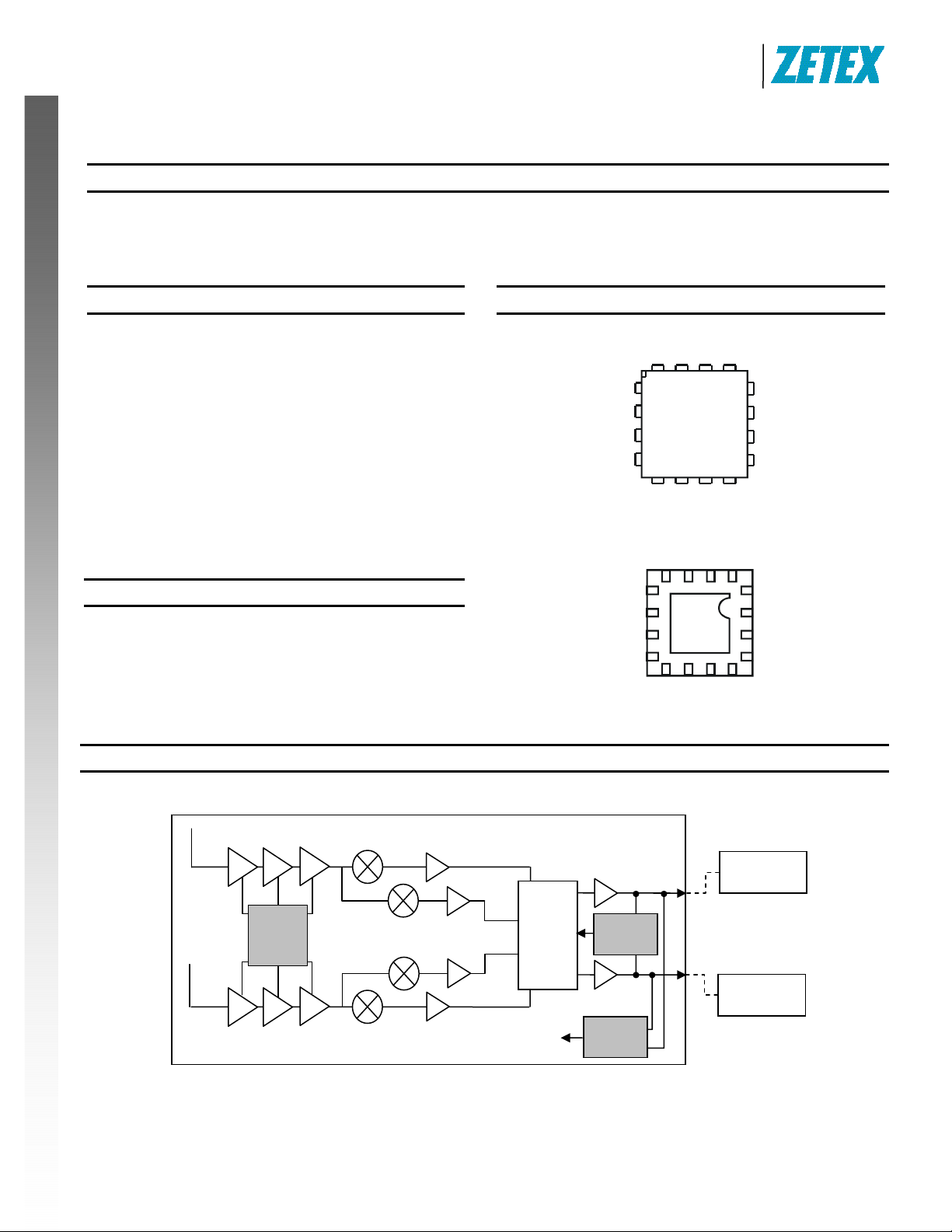
Pin Assignments
BTD1
BTD2
TD2
VCC
HOR1
BHOR1
ENA2
HOR2
BHOR2
Top View
GND
Bottom View
ENA1
FIN1TD1
VPOL1
VPOL2
FIN2
GND
Twin Universal LNB System Diagram
RF Gain Stages
GaAs FET’s
ZABG
Series
Down
Conversion
ZLNB2016
Document number: DS32073 Rev. 1 - 2
IF Gain IF Switching IF Gain,
LNB Control &
Power Mgt.
4x2
MUX
Vout
1 of 7
www.diodes.com
ZLNB
2016
ZLPM
Series
Set-top box
Receiver 1
Set-top box
Receiver 2
February 2010
© Diodes Incorporated

A
f
Device Description
The ZLNB2016 dual polarization and tone switch controller is
one of a wide range of satellite receiver LNB support circuits
available from Diodes Incorporated. It features two
completely independent channels, each providing logic
outputs to control LNB polarization selection, local oscillator
selection and down feed disable. It’s intended to be use d in
voltage and tone controlled LNBs and satellite distribution
systems, replacing many discrete components to save both
manufacturing cost and PCB size whilst improving reliability.
The ZLNB2016 has been designed to be compatible in low
power consumption LNBs so to improve efficiency it
operates from a single supply of 3V to 8V and has a
quiescent current typically of only 2mA. The quiescent
current does not change significantly with load or logic state.
The two polarization control inputs of the Z LNB2016 have a
nominal threshold of 14.75V and the threshol d is guarantee d
over the range of 14.0V to 15.5V. The threshold is
temperature compensated to minimize drift and it also has a
high rejection against the tone signal making the detector
very accurate without the need of further external filtering.
NEW PRODUCT
Each features a low and stable input current that enables
transient protection to be achieved with the addition of only a
single resistor per channel. Multi Feed LNBs can be called to
operate with one or more of their controlling receivers
powered down or disconnected, with attendant cable
mismatch problems.
Product Line o
Diodes Incorporated
ZLNB2016
To ease design for this situation, each polarization input of the
ZLNB2016 has a second threshold set at a nomi nal of 8V. An
input voltage below this threshold indicates “receiver not
present”, and switches the relevant Ena output low. This logic
output can be used to disable the associated down feed
driver, eliminating any problems due to cable mismatch.
Universal LNB local oscillator selection is achieved by
detection of a low level AC voltage superimposed on the
polarization control voltage. To facilitate this function, the
ZLNB2016 includes a separate tone detector for each
channel. Control of detector bandwidth and sensitivity is
provided using an external resistor and capacitor for each
channel. The tone detector has been designed give excellent
rejection of low frequency control signals and DiSEqC™ tone
bursts. The ZLNB2016 has been specifically designed to
minimize the solution cost whilst being flexible. The
ZLNB2016 only requires two external components per
channel to give full user control and functionality. The
ZLNB2016 also includes complimentary outputs so that it can
directly drive many multiplexer ICs without the need of
inverters. Any unused outputs can be left open circuit without
any effect to the remaining circuits operation polarization
switch and tone detector outputs can directly drive TT L and
CMOS logic, pin diodes, IF-amp supply switching and
multiplexer ICs.
ZLNB2016
Document number: DS32073 Rev. 1 - 2
2 of 7
www.diodes.com
February 2010
© Diodes Incorporated

A
Product Line o
f
Diodes Incorporated
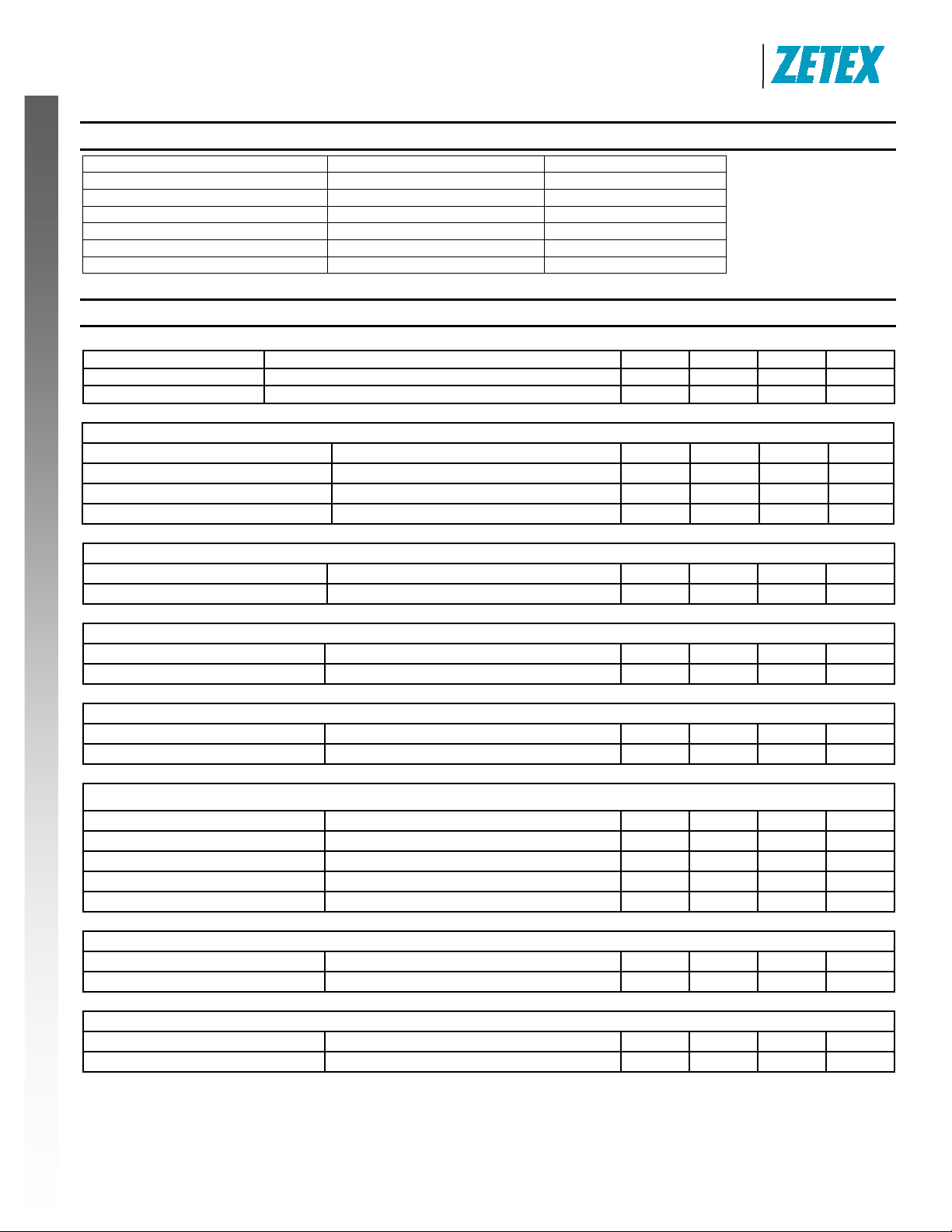
Maximum Ratings
Parameter Rating Unit
Supply Voltage -0.6 to +10 Continuous V
Supply Current 50 mA
V
1, 2 Input Voltage (Note 1) 25 V
POL
Power Dissipation 500 mW
Operating Temperature Range -40 to +85 °C
Storage Temperature Range -40 to +150 °C
Electrical Characteristics (at Tamb = 25°C, Vcc = 3.3V unless otherwise specified.
Parameter Conditions Min. Typ. Max. Unit
Operating Voltage Range 3.0 8.0 V
Supply Current All outputs unloaded, any combination of inputs 2.0 3.0 mA
V
1, 2 Inputs (Note 1)
POL
Input Current V
HOR Threshold T
ENA Threshold T
NEW PRODUCT
Switching Speed HOR, BHOR and ENA outputs 1 ms
HOR1, 2 Outputs
Voltage High I
Voltage Low I
BHOR1, 2 Outputs
Voltage High I
Voltage Low I
ENA1, 2 Outputs
Voltage High I
Voltage Low I
FIN 1, 2 Inputs (Using Test Circuit 1)
Bias Voltage I
Input Impedance V
Amplifier Gain V
Voltage Threshold 100 150 300 mV
Switching Delay TD Outputs 3 10 ms
TD1, 2 Outputs (Using Test Circuit 1)
Voltage High I
Voltage Low I
BTD1, 2 Outputs (Using Test Circuit 1)
Voltage High I
Voltage Low I
Notes: 1. V
2. ESD sensitive, handling precautions are recommended.
stimulus applied via 20k resistors. All levels measured on the input to these resistors.
POL
1,2 = 15V 32 42.5 53 uA
POL
= -40 to +85°C 14.0 14.75 15.5 V
AMB
= -40 to +85°C 7.5 8.0 8.5 V
AMB
= -1mA, V
LOAD
= 5mA, V
LOAD
= -1mA, V
LOAD
= 5mA, V
LOAD
= -1mA, V
LOAD
= 5mA, V
LOAD
= 0 1.25 1.74 2.25 V
FIN
= 100mV
FIN
= 100mV
FIN
= -1mA, Tone Enabled VCC-0.5 VCC-0.3 VCC V
LOAD
= 5mA, Tone Disabled 0 0.3 0.5 V
LOAD
= -1mA, Tone Disabled VCC-0.5 VCC-0.3 VCC V
LOAD
= 5mA, Tone Enabled 0 0.3 0.5 V
LOAD
1,2 = 15.5V VCC-0.5 VCC-0.3 VCC V
POL
1,2 = 14.0V 0 0.3 0.5 V
POL
1,2 = 14.0V VCC-0.5 VCC-0.3 VCC V
POL
1,2 = 15.5V 0 0.3 0.5 V
POL
1,2 = 8.5V VCC-0.5 VCC-0.3 VCC V
POL
1,2 = 7.5V 0 0.3 0.5 V
POL
40 kΩ
P/P
50
P/P
ZLNB2016
ZLNB2016
Document number: DS32073 Rev. 1 - 2
3 of 7
www.diodes.com
February 2010
© Diodes Incorporated
 Loading...