

Page 1
A
Product Line o
f
Diodes Incorporated
ZLNB2015
ADVANCED DBS DUAL CHANNEL VOLTAGE AND TO NE DETECTOR
Summary
The ZLNB2015 is a dual channel polarisation (voltage) and band select (tone) detector IC, primarily for satellite applications such
as Low Noise Blocks (LNBs) and satellite distribution systems. An optimised d esign provides a low supply current and a wide
operating voltage whilst increasing performance and reliability. The ZLNB2015 offers excellent interference rejection with
minimal application cost and packaged in the 3x3mm QFN it provides a very small solution.
Features
• Two high accuracy polarisation voltage detection meeting
the most stringent market needs
• Two robust, interference tolerant 22kHz tone detection
(without external signal filtering)
• “No Receiver” detect function for power saving and
isolation control
• Low quiescent supply current, 2mA typical
• Wide operating supply voltage 3V to 8V
• Low external component count minimises application
NEW PRODUCT
cost
• True and inverted outputs to support popular multiplexer
ICs
Application
• Twin Universal LNBs
• Quad Universal LNBs
• Multi Output LNBs
• Satellite Multi-Switches
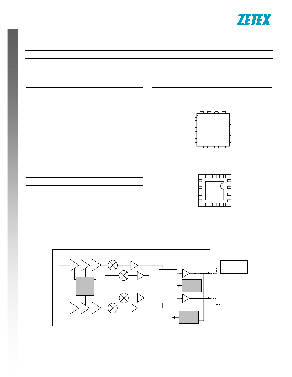
Pin Assignments
BTD1
BTD2
TD2
VCC
HOR1
BHOR1
ENA2
HOR2
BHOR2
Top View
GND
Bottom View
ENA1
FIN1TD1
VPOL1
VPOL2
FIN2
GND
Twin Universal LNB System Diagram
RF Gain Stages
GaAs FET’s
ZABG
Series
Down
Conversion
ZLNB2015
Document number: DS32061 Rev. 1 - 2
IF Gain IF Switching IF Gain,
LNB Control &
Power Mgt.
4x2
MUX
Vout
1 of 7
www.diodes.com
ZLNB
2015
ZLPM
Series
Set-top box
Receiver 1
Set-top box
Receiver 2
January 2010
© Diodes Incorporated
Page 2

A
Product Line o
f
Diodes Incorporated
ZLNB2015
Device Description
The ZLNB2015 dual polarization and tone switch controller is
one of a wide range of satellite receiver LNB support circuits
available from Diodes Incorporated. It features two
completely independent channels, each providing logic
outputs to control LNB polarization selection, local oscillator
selection and downfeed disable. It is intended use is in
American voltage and tone controlled LNBs as well as high
performance Twin, Quad and multiple feed Universal type
LNBs, replacing many discrete components to save both
manufacturing cost and PCB size whilst improving reliability.
The ZLNB2015 has been designed to be compatible in low
power consumption LNBs so to improve efficiency it
operates from a single supply of 3V to 8V and has a
quiescent current typically of only 2mA. The quiescent
current does not change significantly with load or logic state.
The two highly accurate polarization control inputs of the
ZLNB2015 have a nominal threshold of 14.25V and to meet
the required demanding needs of broadcasters they have a
guaranteed threshold range of 14.0V to 14.5V. The threshold
is temperature compensated to minimize drift and it also has
NEW PRODUCT
a high rejection against the tone signal making the detector
very accurate without the need of further external filtering.
Each features a low and stable input current that enables
transient protection to be achieved with the addition of only a
single resistor per channel. Multi Feed LNBs can be called to
operate with one or more of their controlling receivers
powered down or disconnected, with attendant cable
mismatch problems.
ZLNB2015
Document number: DS32061 Rev. 1 - 2
www.diodes.com
To ease design for this situation, each polarization input of the
ZLNB2015 has a second threshold set at a nomi nal of 8V. An
input voltage below this threshold indicates “receiver not
present”, and switches the relevant Ena output low. This logic
output can be used to disable the associated downfeed driv er,
eliminating any problems due to cable mismatch.
Universal LNB local oscillator selection is achieved by
detection of a low level AC voltage superimposed on the
polarization control voltage. To facilitate this function, the
ZLNB2015 includes a separate tone detector for each
channel. Control of detector bandwidth and sensitivity is
provided using an external resistor and capacitor for each
channel. The tone detector has been designed give excellent
rejection of low frequency control signals and DiSEqC™ tone
bursts. The ZLNB2015 has been specifically designed to
minimize the solution cost whilst being flexible. The
ZLNB2015 only requires two external components per
channel to give full user control and functionality. The
ZLNB2015 also includes complimentary outputs so that it can
directly drive many multiplexer ICs without the need of
inverters. Any unused outputs can be left open circuit without
any effect to the remaining circuits operation polarization
switch and tone detector outputs can directly drive TT L and
CMOS logic, pin diodes, IF-amp supply switching and
multiplexer ICs.
2 of 7
January 2010
© Diodes Incorporated
Page 3
A
Product Line o
f
Diodes Incorporated
ZLNB2015
Maximum Ratings
Parameter Rating Unit
Supply Voltage -0.6 to +10 Continuous V
Supply Current 50 mA
V
1, 2 Input Voltage (Note 1) 25 V
POL
Power Dissipation 500 mW
Operating Temperature Range -40 to +85 °C
Storage Temperature Range -40 to +150 °C
Electrical Characteristics (at Tamb = 25°C, Vcc = 3.3V unless otherwise specified.
Parameter Conditions Min. Typ. Max. Unit
Operating Voltage Range 3.0 8.0 V
Supply Current All outputs unloaded, any combination of inputs 2.0 3.0 mA
V
1, 2 Inputs (Note 1)
POL
Input Current V
HOR Threshold T
NEW PRODUCT
ENA Threshold T
Switching Speed HOR, BHOR and ENA outputs 1 ms
HOR1, 2 Outputs
Voltage High I
Voltage Low I
BHOR1, 2 Outputs
Voltage High I
Voltage Low I
ENA1, 2 Outputs
Voltage High I
Voltage Low I
FIN 1, 2 Inputs (Using Test Circuit 1)
Bias Voltage I
Input Impedance V
Amplifier Gain V
Voltage Threshold 100 150 300 mV
Switching Delay TD Outputs 3 10 ms
TD1, 2 Outputs (Using Test Circuit 1)
Voltage High I
Voltage Low I
BTD1, 2 Outputs (Using Test Circuit 1)
Voltage High I
Voltage Low I
Notes: 1. V
2. ESD sensitive, handling precautions are recommended.
stimulus applied via 6.8k resistors. All levels measured on the input to these resistors.
POL
ZLNB2015
Document number: DS32061 Rev. 1 - 2
1,2 = 15V 32 42.5 53 uA
POL
= -40 to +85°C 14.0 14.25 14.5 V
AMB
= -40 to +85°C 7.5 8.0 8.5 V
AMB
= -1mA, V
LOAD
= 5mA, V
LOAD
= -1mA, V
LOAD
= 5mA, V
LOAD
= -1mA, V
LOAD
= 5mA, V
LOAD
= 0 1.25 1.74 2.25 V
FIN
= 100mV
FIN
= 100mV
FIN
= -1mA, Tone Enabled VCC-0.5 VCC-0.3 VCC V
LOAD
= 5mA, Tone Disabled 0 0.3 0.5 V
LOAD
= -1mA, Tone Disabled VCC-0.5 VCC-0.3 VCC V
LOAD
= 5mA, Tone Enabled 0 0.3 0.5 V
LOAD
1,2 = 14.5V VCC-0.5 VCC-0.3 VCC V
POL
1,2 = 14.0V 0 0.3 0.5 V
POL
1,2 = 14.0V VCC-0.5 VCC-0.3 VCC V
POL
1,2 = 14.5V 0 0.3 0.5 V
POL
1,2 = 8.5V VCC-0.5 VCC-0.3 VCC V
POL
1,2 = 7.5V 0 0.3 0.5 V
POL
40 kΩ
P/P
50
P/P
3 of 7
www.diodes.com
January 2010
© Diodes Incorporated
Page 4

A
f
Test Circuit
NEW PRODUCT
BTD1
BTD2
TD2
Note 1: V2 Characteristics
BHOR1
HOR1
VCC
ENA1
FIN1TD1
ZLNB2015
BHOR2
HOR2
ENA2
Type:- AC source
Frequency:- 22kHz
Voltage:- 300mVp/p Enabled
Zero Disabled
VPOL1
VPOL2
FIN2
GND
CF1
CF2
180pF
180pF
Product Line o
Diodes Incorporated
RP1
RP2
6.8k
Switching Delays
6.8k
V2
(See Note 1)
ZLNB2015
V1
3.3V
Tone Input (V2)
TD Outputs
ZLNB2015
Document number: DS32061 Rev. 1 - 2
4 of 7
www.diodes.com
January 2010
© Diodes Incorporated
Page 5

A
Product Line o
f
Diodes Incorporated
ZLNB2015
Applications Information
Above is a partial applications circuit for the ZLNB2015 showing all external components needed for a t ypical twin LNB design.
NEW PRODUCT
The inputs Vpol1 and Vpol2 are design ed to be wired to the power i nputs of the LNB via ESD protection resistors (6.8k). These
inputs control the HOR1/2, BHOR1/2 and ENA1/2 logic outputs. The HOR outputs will be lo w when their correspond ing Vpol i nput
is at or below 14V and high when Vpol is at or a bove 14.5V. The BHOR outputs give inverted versions of their related HOR
outputs. The HOR/BHOR outputs are intended to activate polarisation selection circuitry within an LNB, under control of the LNB
supply voltage. The ENA1/2 outputs are set high when their correspondin g Vpol input is at or above 8.5 V and lo w when Vpol is at
or below 7.5V. These logic outputs can be used to dis able any LNB RF output connected to a receiver (STB) that has been
powered down or disconnected (and hence not providing correct cable matching).
The ZLNB2015 includes circuitry necessary to detect the presence of a 22kHz tone modulated on eit her of two supply inputs to
the LNB. These detectors control the TD1/2 and BTD1/2 outputs. The TD outputs ar e set high on detect ion of a valid tone on their
corresponding LNB input and low in the absence of a tone. The BTD outputs give an inverted versi on of their corresponding TD
outputs. The main elements of each tone detector are an amplifier, a ba nd-pass filter, a rectifier/smoother a nd a com parator. User
control is given over the gain of the amplifier and the lower frequenc y limit of the filter, using an external resistor and capacitor.
(The ESD protection resistor noted above can be used to set amplifier gain, hence requiring only one component for both
functions.) The higher frequency limit of the filter is set internall y to block signals above 100kHz. T he comparator circu it utilises no
external components.
The HOR, BHOR, TD, BTD and ENA outputs are designed to be compatibl e with LSTTL, CMOS and common MIMIC multiple xer
loads. Any input or output that is not required can be left open circuit.
BTD1
BTD2
TD2
BHOR1
HOR1
ZLNB2015
BHOR2
HOR2
VCC
ENA1
180pF
FIN1TD1
VPOL1
VPOL2
FIN2
ENA2
GND
C1
C2
180pF
R2
6.8k
R1
Downfeed 1
6.8k
Downfeed 2
Output Truth Table
The ZLNB2015 includes two independent channels, each containing a voltage detector and tone detector. The following truth table
applies to each channel.
Tone Vpol TD BTD HOR BHOR ENA
Off 14V Low High Low High High
Off 14.5V Low High High Low High
On 14V High Low Low High High
On 14.5V High Low High Low High
- <7.5V - - Low High Low
ZLNB2015
Document number: DS32061 Rev. 1 - 2
5 of 7
www.diodes.com
January 2010
© Diodes Incorporated
Page 6

A
f
Package Outline Dimensions
Note: Controlling dimensions are in millimeters. Approximate dimensions are provided in inches.
The package appearance may vary as shown, for further details please contact your local Diodes sales office.
NEW PRODUCT
D
Pin #1 ID
e
b
E
E2
Z
A1
A3
A
L
D2
Product Line o
Diodes Incorporated
ZLNB2015
QFN16 3x3
Dim Min Max
A 0.55 0.65
A1 0.00 0.05
A3 0.15 Typ
b 0.18 0.28
D 2.95 3.05
D2 1.40 1.60
e 0.50 BSC
E 2.95 3.05
E2 1.40 1.60
L 0.35 0.45
Z 0.625 Typ
All Dimensions in mm
Ordering Information (Note x)
Device Package
ZLNB2015JA16TC QFN1633 13 8 3000
Reel Size
(inches)
ZLNB2015
Document number: DS32061 Rev. 1 - 2
6 of 7
www.diodes.com
Tape Width
(mm)
Quantity
(per reel)
January 2010
© Diodes Incorporated
Page 7

A
Product Line o
f
Diodes Incorporated
ZLNB2015
DIODES INCORPORATED MAKES NO WARRANTY OF ANY KIND, EXPRESS OR IMPLIED, WITH REGARDS TO THIS DOCUMENT,
INCLUDING, BUT NOT LIMITED TO, THE IMPLIED WARRANTIES OF MERCHANTABILITY AND FITNESS FOR A PARTICULAR PURPOSE
(AND THEIR EQUIVALENTS UNDER THE LAWS OF ANY JURISDICTION).
Diodes Incorporated and its subsidiaries reserve the right to make modifications, enhancements, improvements, corrections or other changes
without further notice to this document and any product described herein. Diodes Incorporated does not assume any liability arising out of the
application or use of this document or any product described herein; neither does Diodes Incorporated convey any license under its patent or
trademark rights, nor the rights of others. Any Customer or user of this document or products described herein in such applications shall assume
all risks of such use and will agree to hold Diodes Incorporated and all the companies whose products are represented on Diodes Incorporated
website, harmless against all damages.
Diodes Incorporated does not warrant or accept any liability whatsoever in respect of any products purchased through unauthorized sales channel.
Should Customers purchase or use Diodes Incorporated products for any unintended or unauthorize d application, Customers shall indemnify and
hold Diodes Incorporated and its representatives harmless against all claims, damages, expenses, and attorney fees arising out of, directly or
indirectly, any claim of personal injury or death associated with such unintended or unauthorized application.
Products described herein may be covered by one or more United States, international or foreign patents pending. Product names and markings
noted herein may also be covered by one or more United States, international or foreign trademarks.
NEW PRODUCT
Diodes Incorporated products are specifically not authorized for use as critical components in life support devices or systems without the express
written approval of the Chief Executive Officer of Diodes Incorporated. As used herein:
A. Life support devices or systems are devices or systems which:
1. are intended to implant into the body, or
labeling can be reasonably expected to result in significant injury to the user.
B. A critical component is any component in a life support device or system whose failure to perform can be reasonably expected to cause the
failure of the life support device or to affect its safety or effectiveness.
Customers represent that they have all necessary expertise in the safety and regulatory ramifications of their life support devices or systems, and
acknowledge and agree that they are solely responsible for all legal, regulatory and safety-related requirements concerning their products and any
use of Diodes Incorporated products in such safety-critical, life support devices or systems, notwithstanding any devices- or systems-related
information or support that may be provided by Diodes Incorporated. Further, Customers must fully indemnify Diodes Incorporated and its
representatives against any damages arising out of the use of Diodes Incorporated products in such safety-critical, life support devices or systems.
Copyright © 2010, Diodes Incorporated
www.diodes.com
2. support or sustain life and whose failure to perform when properly used in accordance with instructions for use provided in the
IMPORTANT NOTICE
LIFE SUPPORT
ZLNB2015
Document number: DS32061 Rev. 1 - 2
7 of 7
www.diodes.com
January 2010
© Diodes Incorporated
 Loading...