

Page 1

DUAL TONE AND POLARITY SWITCH
LNB MULTIPLEX CONTROLLER
DEVICE DESCRIPTION
The ZLNB2012 dual polarisation and tone switch
controller is one of a wide range of satellite receiver
LNB support circuits available from Zetex. It features
two completely independent channels, each providing
logic outputs to control LNB polarisation selection,
local oscillator selection and downfeed disable. It is
intended for use in Twin, Quad and multiple feed
Universal LNBs, replacing many discrete components
to save both manufacturing cost and PCB size whilst
improving reliability.
The two highly accurate polarisation control inputs of
the ZLNB2012 have a nominal threshold of 14.25V and
to meet the required demanding needs from some
broadcasters they have a switching range of 14.0V to
14.5V. The threshold is temperature compensated to
minimise drift. Each features a low and stable input
current that enables transient protection to be
achieved with the addition of only a single resistor per
channel.
Multi Feed LNBs can be called to operate with one or
more of their controlling receivers powered
down/disconnected, with attendant cable mismatch
problems. To ease design for this situation, each
polarisation input of the ZLNB2012 has a second
threshold set at 9V. An input voltage below this
threshold indicates“ receiver not present”, and
switches the relevant control channels high. This logic
output canbeused to disable the associateddownfeed
driver, eliminating any problems due to cable
mismatch.
ZLNB2012
Universal LNB local oscillator selection is achieved by
detection of a low level AC voltage superimposed on
the polarisation control voltage. To facilitate this
function, the ZLNB2012 includes a separate tone
detector for each channel. Control of detector
bandwidth and sensitivity is provided using an
external resistor and capacitor for each channel. The
tone detector has been designed give excellent
rejection of low frequency control signals and
DiSEqC™ tone bursts.
The ZLNB2012 has been specifically designed to
minimise the solution cost whilst being flexible. The
ZLNB2012 only requires two external components per
channel to give full user control and functionality. The
ZLNB2012 also includes complimentary outputs so
that it can directly drive many multiplexer IC’s without
the need of an inverter. Any unused outputs can be left
open circuit without any effect to the remaining circuits
operation Polarisation switch and tone detector
outputs can directly drive TTL and CMOS logic, pin
diodes, IF-amp supply switching and multiplexer IC’s.
The ZLNB2012 operates from a single supply which
can be anything from 5-8V. Its quiescent current is
typically only 9mA and this does not change
significantly with loadorlogicstate.It is availablein the
space saving QSOP16 surface mount package.
FEATURES
·
Dual polarisation and tone switch
·
Reduced Cost Solution, only 2 external components
per channel
·
Close tolerance (14-14.5V) and temperature
compensated polarisation switch
·
Multiplexer IC direct drive
·
Tone andpol.Outputs are TTL, CMOS,Pindiode and
IF amp capable
·
Transient resistant inputs
·
Includes Receiver-Off detector
·
User adjustable filter centre frequency and
bandwidth
PROVISIONAL ISSUE A - OCTOBER 2001
·
Low frequency and DiSEqC control signals
rejection
·
Eliminates many close tolerance discrete
components
·
Wide supply operating range
·
Low quiescent current
APPLICATIONS
·
Twin Universal LNB’s
·
Quad Universal LNB’s
·
Multi Feed Universal LNB’s
·
LNB switch boxes
1
Page 2
ZLNB2012
ABSOLUTE MAXIMUM RATINGS
Supply Voltage -0.6V to 12V
Supply Current 500mA
V
and V
POL1
Input Voltage 25V Continous
Operating Temperature -40 to 80°C
Storage Temperature -40 to 85°C
POL2
Power Dissipation (T
amb 25 C)
QSOP16 500mW
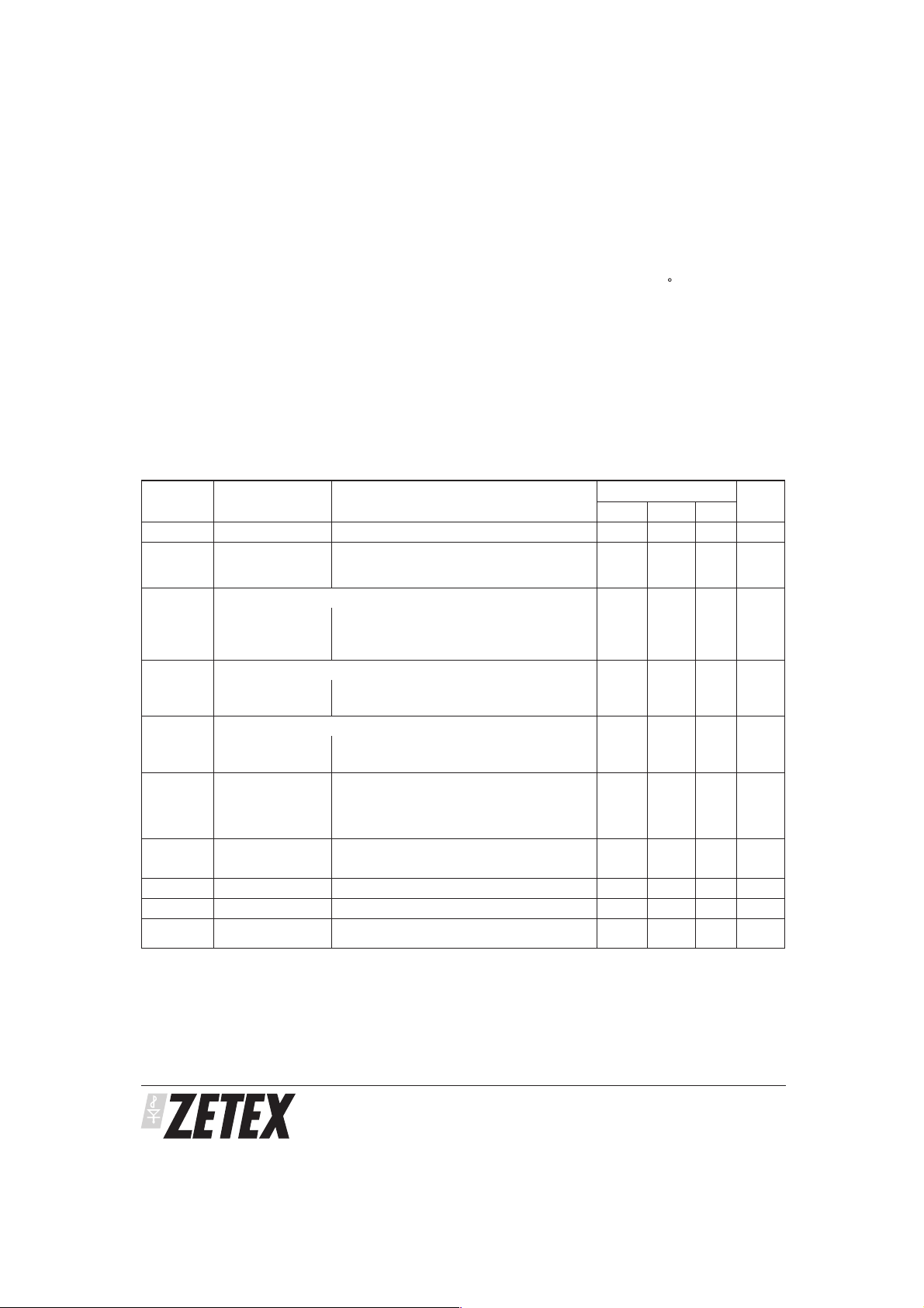
ELECTRICAL CHARACTERISTICS TEST CONDITIONS (Unless otherwise stated):
T
amb= 25⬚C,VCC
SYMBOL PA RAMETER CONDITIONS
V
CC
I
CC
I
POL
V
TPOL
T
SPOL
VHOR
HIGH
VHOR
LOW
VBHOR
HIGH
VBHOR
LOW
VEN
HIGH
VEN
LOW
V
OUT
F
inz
AG Amplifier Gain V
FV
T
=5V
LIMITS
Min Typ Max
Supply Voltage 5 8 V
Supply Current HOR1,2= BHOR1,2= TD1,2= BTD1, 2= 0mA
1= V
2= Don’t Care
POL
= 25V (Note 2)
=-40°C to 80°C
1,2=-100A,V
OUT
1,2=5mA,V
OUT
2 Outputs
1,2=-100A,V
OUT
1,2=5mA,V
OUT
POL
POL
POL
POL
POL
1,2=14V
1,2=14.5V
1,2=14.0V
POL
1,2=14.5V
1,2=10V
1,2=8.0V
and V
V
POL1
POL2
Inputs
Current
Threshold Voltage
Switching Speed
HOR
1 and HOR
OUT
Voltage High
Voltage Low
BHOR
1 and BHOR
OUT
Voltage High
Voltage Low
Enable 1,2
Outputs
Voltage High
Voltage Low
V
POL
1= FIN2= Don’t Care
F
IN
V
POL1=VPOL2
T
amb
2 Outputs
OUT
IHOR
IHOR
OUT
IBHOR
IBHOR
IEnable 1,2=-100A,V
IEnable 1,2=500A,V
Filter Amplifier
3
I
Bias Voltage
Input Impedance V
V Threshold
3
=0 1.75 1.95 2.15 V
fin
=100mV p/p 150 ⍀
FIN
=100mV p/p 30 V/mA
FIN
10014200
V
V
V
100 170 350 mV
912mA
14.25
-1.00VCC0.7
CC
0.30
-1.00VCC0.7
CC
0.30
-1.00VCC0.7
CC
0.30
240
14.5
100
V
CC
0.5
V
CC
0.5
V
CC
0.5VV
UNITS
A
V
S
V
V
V
V
p/p
Note:-
1) The parameters Filter AmplifierV
related to Vcc.
OUT,IOUT
2) Applied via 1k resistors
3) These parameters are linear related to V
, Rectifier V
CC
and Comparator Threshold Voltage areall directly (linearly)
OUT
PROVISIONAL ISSUE A - OCTOBER 2001
2
Page 3

ZLNB2012
ELECTRICAL CHARACTERISTICS TEST CONDITIONS (Unless otherwise stated):
T
amb= 25⬚C,VCC
SYMBOL PA RAMETER CONDITIONS
V
VHIGH
V
VLOW
V
VHIGH
V
VLOW
Note:-
1) Theparameters Filter Amplifier V
related to Vcc.
2) Applied via 1k resistors
3) These parameters are linear related to V
=5V
TD 1,2 Outputs
Voltage high
Voltage Low
BTD 1,2 Outputs
Voltage high
Voltage Low
ITD 1,2=-100A, Test Circuit 1,
Tone enabled
ITD 1,2=15mA, Test Circuit 1,
Tone disabled
IBTD 1,2=-100A, Test Circuit 1,
Tone disabled
IBTD 1,2=15mA, Test Circuit 1,
Tone enabled
OUT,IOUT
, RectifierV
CC
and ComparatorThreshold Voltage are all directly(linearly)
OUT
LIMITS
Min Typ Max
-1.00VCC-0.7
V
CC
0.3
-1.00VCC-0.7
V
CC
0.3
V
CC
0.5VV
V
CC
0.5VV
UNITS
PROVISIONAL ISSUE A - OCTOBER 2001
3
Page 4

ZLNB2012
TEST CIRCUIT 1 (ZLNB2012 Pinout for QSOP16 package designator - Q16)
CF2
10nF
RP2
1.0k
BTD2
TD2
BHOR2
HOR2
ENA2
GND
FIN2
1
BTD1
TD1
BHOR1
HOR1
VCC
ENA1
FIN1
VPOL2 VPOL1
V1
5V
10nF
CF1
RP1
1.0k
V2
(See Note 1)
Note 1: V2 Characteristics
Type:- AC source
Frequency:- 22kHz
Voltage:- 300mVp/p Enabled
Zero Disabled
Tone Input (V2)
TD Outputs
Switching Delays
PROVISIONAL ISSUE A - OCTOBER 2001
4
Page 5

ZLNB2012
The following diagram shows a typical block diagram
for a twin universal LNB design. The ZLNB2012 device
provides the two polarity and two tone switches
required to decode the two independent receiver
feeds. Thedevice is also able todetect the absence of a
revceiver connection to either port of the LNB
providing all outputs to go high hence disabling of the
port. This allows the avoidance of unwanted signal
reflections from an unterminated down feed cable.
Horizontal
Antenna
Gain Stage
GaAs/HEMTFET
High Band
+
1
3
Mixer
+
Low Band
ASTRA
10.95 GHz-11.7 GHz
Standard Band
10.7 GHz-11.8 GHz
Enhanced Band
Bias Generator
ZNBG40XX
Series
Low Band
igh Band
H
High Band
+
4
Mixer
+
Low Band
Vertical
Antenna
2
Gain Stage
GaAs/HEMTFET
Additionally the frontend biasrequirements of theLNB
are providedby theZNBG4000 or ZNBG6000 offering a
very efficient and cost effective solution
Control Input
<=13V-Horizontal
>=14.5V-Vertical
ZLNB2012 Series
Dual H/V Switch
22kHz Switch
High Band
Horizontal
Low Band
Horizontal
PIN
Diode
&
Control
High Band
Vertical
Low Band
Vertical
MUX
DC Input
13-25V
H/V Output 1
IF down feed
950-1750 MHz
- Standard Band
950-2050 MHz
- Enhanced Band
H/V Output 2
PROVISIONAL ISSUE A - OCTOBER 2001
5
Page 6

ZLNB2012
APPLICATION CIRCUIT EXAMPLES
The following circuit shows the additional components that will be used for polarisation mode and 22kHz tone
detection in typical ZLNB2012 application (ZLNB2012 Pinout for QSOP16 package designator - Q16).
1
RP2
1.0k
LNB Downfeed No.2
CF2
10nF
BTD2
TD2
BHOR2
HOR2
ENA2
GND
FIN2
VPOL2 VPOL1
BTD1
TD1
BHOR1
HOR1
VCC
ENA1
FIN1
CF1
10nF
Vcc
RP1
1.0k
LNB Downfeed No.1
ZLNB2012 PINOUT FOR QSOP16
PACKAGE DESIGNATOR - Q16
1
BTD2
TD2
BHOR2
HOR2
ENA2
GND
FIN2
VPOL2 VPOL1
BTD1
TD1
BHOR1
HOR1
VCC
ENA1
FIN1
ORDERING INFORMATION
Part Number Package Part Mark
ZLNB2012Q16 QSOP16 ZLNB2012
SAMPLE ORDERING INFORMATION
Part Number Package Part Mark
#ZLNB2012Q16 QSOP16 ZLNB2012
PROVISIONAL ISSUE A - OCTOBER 2001
6
Page 7

FURTHER INFORMATION
Inputs Vpol1 and Vpol2 aredesigned to bewired to the
power inputs of an LNB via a high value (1K) resistors.
Input Vpol1 controls outputs HOR1, BHOR1 and ENA1.
Input Vpol2 controls outputs HOR2, BHOR2 and ENA2.
With either input voltage set at or below 14V, the
corresponding HOR pin will be active and the
corresponding BHOR pin will be the inverse of HOR.
With either input voltage at 14.5V or higher, the
corresponding HOR pin will be active and the
corresponding BHOR pin will be the inverse. Should
the voltage applied to either Vpol input fall below 8V,
the corresponding ENA (enable) pin will be low,
otherwise these outputs will remain high. Any input or
output may be left open circuit without any effect on
the remaining circuitry.
The ZLNB2012 includes all the circuitry necessary to
detect the presence of a 22kHz tone modulated on the
supply input to the LNB. The main elements of the
detector are an op-amp, a rectifier/smoother and a
comparitor. The op-amp has a pre-set internal
feedback resistor so that just a simple RC network
wired to the input gives user defined gain and low
frequency cut filter characteristics.
Output Truth Table
ZLNB2012
The RC network components also serve two other
purposes. The resistor provides overvoltage
protection for theVpol pinand thecapacitor minimises
tone interference of the Vpol threshold. The upper
frequency roll-off ofthe op-amphas beenset internally
at above 100kHz to allow the amplifier to be used with
other common tone switch frequencies.
The rectifier/smoother/comparitor function is provided
by a complex propriety circuit that allows the
ZLNB2012 to reliably detect wanted tones whilst
ignoring low frequency square wave switch box
signals, DiSEqC™ bursts and supply switching
transients common when using DiSEqC-2™ ready
set-top boxes. This is all achieved without the need for
any further external components. The threshold of the
comparitor is supply dependent, hence the gain of the
preceding op-amp mustbe adjustedin linewith supply
voltage.
The ZLNB2012 includes two independent channels, each containing a voltage detector and tone detector. The
following truth table applies to each channel:-
Tone Vpol TD BTD HOR BHOR ENA
Off ⭐14V Low High Low High High
Off ⭓14.5V Low High High Low High
On ⭐ 14V High Low Low High High
On ⭓14.5V High Low High Low High
- <8V - - Low High Low
PROVISIONAL ISSUE A - OCTOBER 2001
7
Page 8

ZLNB2012
PACKAGE DIMENSIONS
QSOP16
DIM Millimetres Inches
MIN MAX MIN MAX
A 4.80 4.98 0.189 0.196
B 0.635 0.025 NOM
C 0.23 REF 0.009 REF
D 0.20 0.30 0.008 0.012
E 3.81 3.99 0.15 0.157
F 1.35 1.75 0.053 0.069
G 0.10 0.25 0.004 0.01
J 5.79 6.20 0.228 0.244
K0° 8° 0° 8°
© Zetex plc 2001
Zetex plc
Fields New Road
Chadderton
Oldham, OL9 8NP
United Kingdom
Telephone (44) 161 622 4422
Fax: (44) 161 622 4420
These offices are supported by agents and distributors in major countries world-wide.
This publication is issued to provide outline information only which (unless agreed by the Company in writing) may not be used, applied or
reproduced for any purpose or form part of any order or contract or be regarded as a representation relating to the products or services
concerned. The Company reserves the right to alter without notice the specification, design, price or conditions of supply of any product or
service.
For the latest product information, log on to
Zetex GmbH
Streitfeldstraße 19
D-81673 München
Germany
Telefon: (49) 89 45 49 49 0
Fax: (49) 89 45 49 49 49
www.zetex.com
Zetex Inc
700 Veterans Memorial Hwy
Hauppauge, NY11788
USA
Telephone: (631) 360 2222
Fax: (631) 360 8222
Zetex (Asia) Ltd
3701-04 Metroplaza, Tower 1
Hing Fong Road
Kwai Fong, Hong Kong
China
Telephone: (852) 26100 611
Fax: (852) 24250 494
PROVISIONAL ISSUE A - OCTOBER 2001
8
 Loading...