

Page 1
A
f
Product Line o
Diodes Incorporated
ZLDO1117
1A LOW DROPOUT POSITIVE REGULATOR
1.2V, 1.5V, 1.8V, 2.5V, 3.3V, 5.0V AND ADJUSTABLE OUTPUTS
Description
ZLDO1117 is a low dropout positive adjustable or fixed-mode
regulator with 1A output current capability.
The ZLDO1117 has a 2% tolerance across the industrial temperature
range and is guaranteed to have lower than 1.2V dropout at full load
current making it ideal to provide well-regulated outputs of 1.2V to
5.0V with input supply voltages up to 18V.
The ZLDO1117 is ideally suited to provide well-regulated supplies for
low voltage IC applications such as high-speed bus termination and
low current 3.3V logic supply across the whole industrial temperature
range.
Features
• 1.2V Maximum Dropout at Full Load Current
• 2% Tolerance Over Temperature, Line and Load Variations
• Fast Transient Response
• Output Current Limiting
• Built-in Thermal Shutdown
• Good Noise Rejection
• Suitable for use with MLCC Capacitors
• Qualified to AEC-Q100 Grade 2 (see ‘Ordering Information’)
• PPAP capable (Note 4)
• -40 to +125°C Junction Temperature Range
• Available in TO252 and SOT223 with “Green” Molding Compound
(No Br, Sb)
Lead-Free Finish; RoHS Compliant (Notes 1 & 2)
Halogen and Antimony Free. “Green” Device (Note 3)
Notes: 1. EU Directive 2002/95/EC (RoHS) & 2011/65/EU (RoHS 2) compliant. All applicable RoHS exemptions applied.
2. See http://www.diodes.com for more information about Diodes Incorporated’s definitions of Halogen- and Antimony-free, "Green" and Lead-free.
3. Halogen- and Antimony-free "Green” products are defined as those which contain <900ppm bromine, <900ppm chlorine (<1500ppm total Br + Cl)
and <1000ppm antimony compounds.
4. Automotive products are AEC-Q100 qualified and are PPAP capable. Automotive, AEC-Q100 and standard products are electrically and thermally
the same, except where specified.
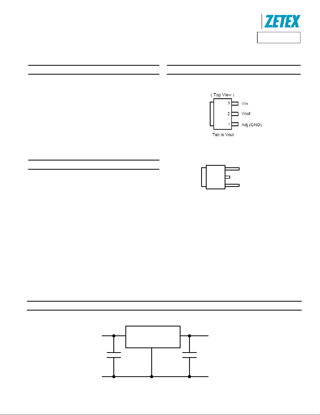
Pin Assignments
(Top View)
3
2
1
Tab is Vout
SOT223
TO252
Vin
Vout
Adj (GND)
Typical Applications Circuit
1A I/O – 1.8V Core Regulator
3.3V
ZLDO1117-18
1.8V
4.7µF
MLCC
4.7µF
MLCC
ZLDO1117
Document number: DS32018 Rev. 6 - 2
1 of 14
www.diodes.com
July 2012
© Diodes Incorporated
Page 2
A
f
Product Line o
Diodes Incorporated
ZLDO1117
Pin Descriptions
Pin
Name
Adj (GND) I 1
V
O 2
OUT
VIN I 3
I/O
Pin
Number
Function
A resistor divider from this pin to the V
Fixed-Mode).
The output of the regulator. A minimum of 4.7µF capacitor (0.05Ω ≤ ESR ≤ 0.5Ω) must be connected
from this pin to ground to insure stability. For improved ac load response a larger output capacitor is
recommended.
The input pin of regulator. Typically a large storage capacitor (0.05Ω ≤ ESR ≤ 0.5Ω) is connected from
this pin to ground to ensure that the input voltage does not sag below the minimum dropout voltage
during the load transient response. This pin must always be 1.3V higher than V
device to regulate properly.
pin and ground sets the output voltage (Ground only for
OUT
in order for the
OUT
Absolute Maximum Ratings (@T
= +25°C, unless otherwise specified.)
A
Symbol Parameter Rating Unit
VIN Input Supply Voltage (Relative to Ground) -0.03 to +18 V
TJ Junction Temperature +150 °C
Power Dissipation See SOA Curve
TST Storage Temperature -65 to +150 °C
Unless otherwise stated voltages specified are relative to the ANODE pin.
1.2
1
0.8
(A)
0.6
LOAD
I
0.4
SOA
ESD Susceptibility
Symbol Parameter Rating Unit
HBM Human Body Model 4 kV
MM Machine Model 400 V
Stresses greater than the 'Absolute Maximum Ratings' specified above, may cause permanent damage to the device. These are stress ratings only; functional
operation of the device at these or any other conditions exceeding those indicated in this specification is not implied. Device reliability may be affected by exposure to
absolute maximum rating conditions for extended periods of time.
Semiconductor devices are ESD sensitive and may be damaged by exposure to ESD events. Suitable ESD precautions should be taken when handling and
transporting these devices
ZLDO1117
Document number: DS32018 Rev. 6 - 2
0.2
0
0 5 10 15 20 25
Safe Operation Area (SOA) Curve
- V
(V)
V
IN
OUT
2 of 14
www.diodes.com
July 2012
© Diodes Incorporated
Page 3
A
f
Product Line o
Diodes Incorporated
ZLDO1117
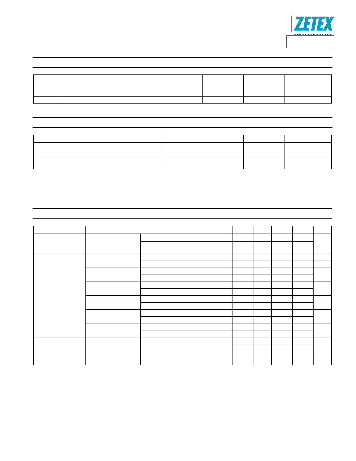
Recommended Operating Conditions (@T
= +25°C, unless otherwise specified.)
A
Symbol Parameter Min Max Unit
VIN Input voltage 2.7 (Note 8) 18 V
IO Output current 0.01 1 A
TJ Operating Junction Temperature Range (Note 5) -40 +125 °C
Package Thermal Data
Thermal Resistance Package Rating Unit
Junction-to-Ambient, θJA
Junction-to-Case, θJC
Notes: 5. ZLDO1117 contains an internal thermal limiting circuit that is designed to protect the regulator in the event that the maximum junction temperature
exceeded. When activated, typically at 150°C, the regulator Output switches off and then back on as the die cools.
6. Test condition for SOT223: T
7. Test condition for TO252: T
8. Ensures correct operation without entering dropout. Device will continue to operate below this minimum input voltage under dropout conditions.
= +27°C, no air flow, device mounted on 2”X2” polyimide PCB, 2 oz copper, 5.6mmX5.6mm pad.
A
= +27°C, no air flow, device mounted on 2”X2” polyimide PCB, 1 oz copper, 2cmX2cm pad.
A
SOT223 (Note 6)
TO252 (Note 7)
SOT223 (Note 6)
TO252 (Note 7)
Electrical Characteristics (@T
= +25°C, unless otherwise specified.)
A
Parameter Conditions TA Min Typ Max Unit
(VIN-V
Reference Voltage ZLDO1117-ADJ
ZLDO1117-1.2
ZLDO1117-1.5
ZLDO1117-1.8
Output Voltage
ZLDO1117-2.5
ZLDO1117-3.3
ZLDO1117-5.0
ZLDO1117-ADJ
Line Regulation
Notes: 9. See thermal regulation specifications for changes in output voltage due to heating effects. Line and load regulation are measured at a constant
junction temperature by low duty cycle pulse testing. Load regulation is measured at the output lead = 1/18” from the package.
10. Line and load regulation are guaranteed up to the maximum power dissipation of 15W. Power dissipation is determined by the difference between input
and output differential and the output current. Guaranteed maximum power dissipation will not be available over the full input/output range.
ZLDO1117-1.2
ZLDO1117-xx
V
10mA < IO< 1A
IO = 10mA, VIN = 3.2V 25 1.188 1.200 1.212 V
10mA< IO< 1A, 2.7V <VIN< 12V FT 1.176 1.224
IO = 10mA, VIN = 3.5V 25 1.485 1.500 1.515
0 < IO< 1A, 2.9V <VIN< 12V FT 1.470 1.530
IO = 10mA, VIN = 3.8V 25 1.782 1.800 1.818
0 < IO< 1A, 3.2V <VIN< 12V FT 1.764 1.836
IO = 10mA, VIN = 4.5V 25 2.475 2.500 2.525
0 < IO< 1A, 3.9V <VIN< 12V FT 2.450 2.550
IO = 10mA, VIN = 5.3V 25 3.267 3.300 3.333
0 < IO< 1A, 4.7V <V
IO = 10mA, VIN = 7V 25 4.95 5.000 5.05
0 < IO< 1A, 6.4V <V
IO = 10mA,
V
IO = 0mA,
V
) = 2V, IO = 10mA 25 1.238 1.250 1.263
OUT
+1.4V < VIN< 10V,
OUT
+1.5V<VIN<12V
OUT
+1.5V<VIN<12V
OUT
< 12V FT 3.235 3.365
IN
< 12V FT 4.900 5.100
IN
FT 1.225 1.275
25 0.1
FT 0.2
25 0.1
FT 0.2
ZLDO1117
Document number: DS32018 Rev. 6 - 2
3 of 14
www.diodes.com
107
73
16
12
°C/W
°C/W
V
V
V
V
V
V
%
%
July 2012
© Diodes Incorporated
Page 4
A
f
Product Line o
Diodes Incorporated
ZLDO1117
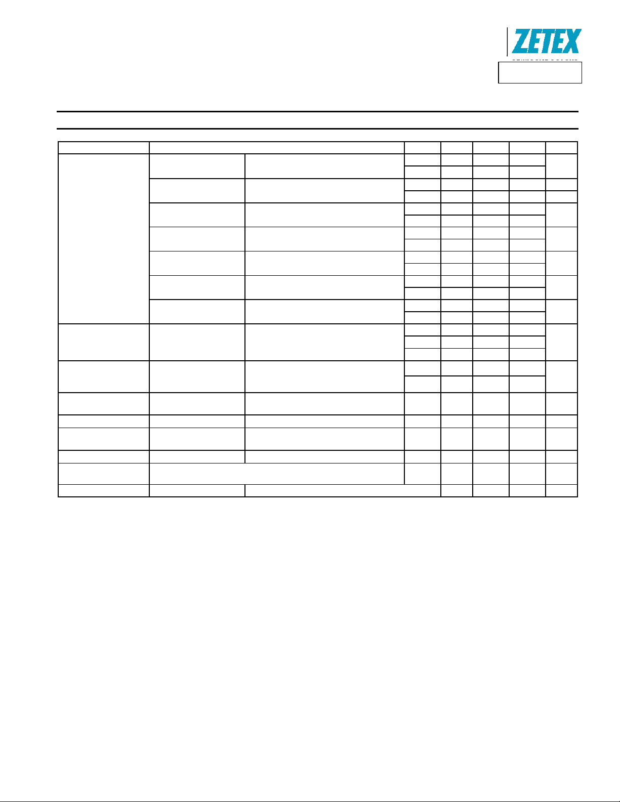
Electrical Characteristics (cont.) (@T
Parameter Conditions TA Min Typ Max Unit
ZLDO1117-ADJ
ZLDO1117-1.2
ZLDO1117-1.5
Load Regulation
Dropout Voltage
(VIN-V
Current Limit
Minimum Load Current
(Note 8)
Quiescent current
GND current
Thermal Regulation
Ripple Rejection
Temperature Stability
Notes: 8. See thermal regulation specifications for changes in output voltage due to heating effects. Line and load regulation are measured at a constant
junctiontemperature by low duty cycle pulse testing. Load regulation is measured at the output lead = 1/18” from the package.
9. Line and load regulation are guaranteed up to the maximum power dissipation of 15W. Power dissipation is determined by the difference between input
and output differential and the output current. Guaranteed maximum power dissipation will not be available over the full input/output range.
OUT
)
ZLDO1117
Document number: DS32018 Rev. 6 - 2
ZLDO1117-1.8
ZLDO1117-2.5
ZLDO1117-3.3
ZLDO1117-5.0
ZLDO1117ADJ/1.2/1.5/1.8/2.5/
3.3/5.0
ZLDO1117-
ADJ/1.2/1.5/1.8/2.5/
3.3/5.0
ZLDO1117-ADJ
ZLDO1117-1.2
ZLDO1117-xx VIN< 18V, IO = 0mA
ZLDO1117-ADJ
ZLDO1117-1.2
30ms pulse
f = 120Hz, C
I
= 100mA, ZLDO1117-XXX VIN = V
OUT
IO = 10mA
= 25µF Tantalum,
OUT
= +25°C, unless otherwise specified.)
A
VIN=3.3V,V
(Notes 9, 10)
VIN=2.7V, 10mA < IO < 1A,
(Notes 9, 10)
VIN = 3V, 0 < IO< 1A,
(Notes 9, 10)
VIN = 3.3V, 0 < IO< 1A,
(Notes 9, 10)
VIN = 4V, 0 < IO< 1A,
(Notes 9, 10)
VIN = 4.8V, 0 < IO< 1A,
(Notes 9, 10)
VIN = 6.5V, 0 < IO< 1A,
(Notes 9, 10)
IO = 1A, ΔV
(VIN-V
VIN = <18V FT 2 5 mA
VIN = 7V FT 35 120 µA
=0, 10mA<IO<1A,
ADJ
= 1%V
OUT
) = 5V
OUT
+3V
OUT
4 of 14
www.diodes.com
OUT
25 0.2
FT
25 0.2 %
FT 0.4
25 3
FT 6
25 4
FT 8
25 5
FT 10
25 6.6
FT 13
25 10
FT 20
25 1.11 1.2
0 ~ 125
FT
25
FT 1. 1
FT 4 10 mA
25 0.1 %/W
25 60 80 dB
0.5 %
0.4
1.3
1.35
© Diodes Incorporated
%
mV
mV
mV
mV
mV
V
A
July 2012
Page 5
A
f
A
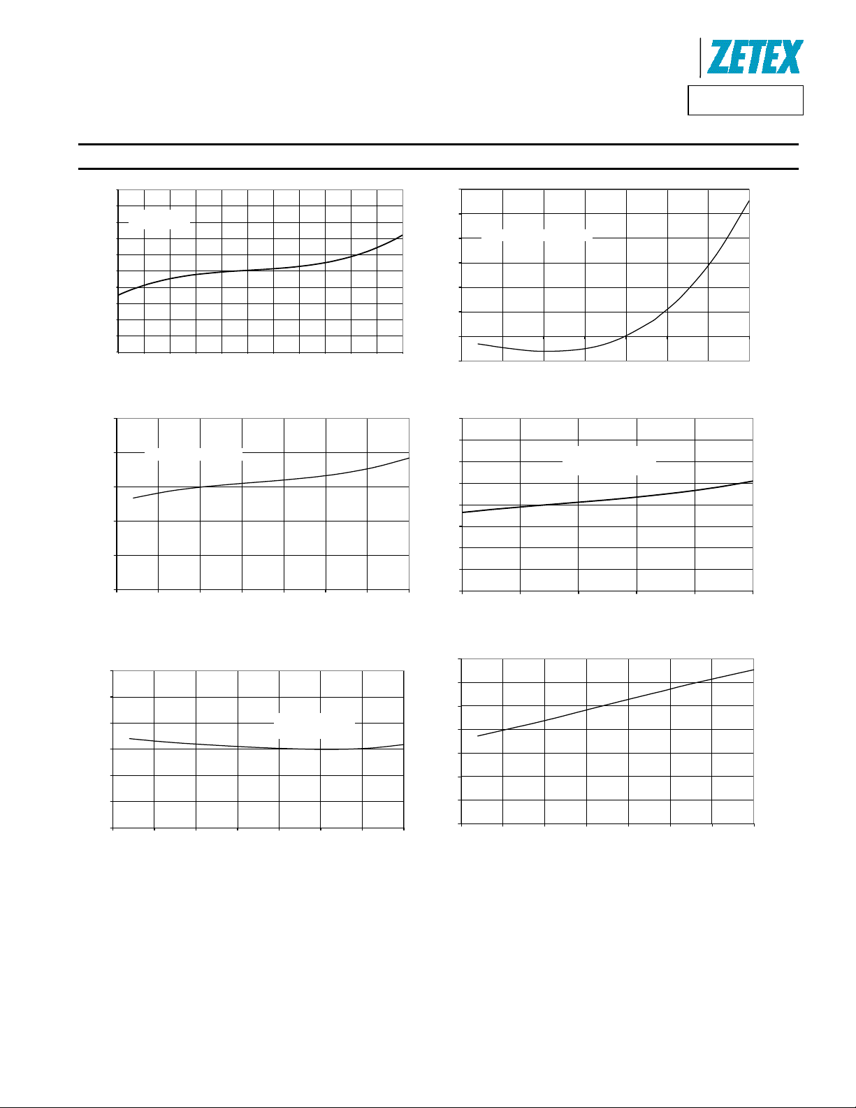
Typical Characteristics
0.5
0.4
Adjustable version
0.3
= 10mA
I
LOAD
0.2
0.1
0
∆Vout (%)
-0.1
-0.2
-0.3
-0.4
-0.5
-40 -25 -10 5 20 35 50 65 80 95 110 125
Output Voltage Variation vs. Temperature Line Regulation vs. Temperature
0.25
0.2
0.15
0.1
Load Regulation (%)
0.05
VIN=3.3V, 10mA<I
0
-50 -25 0 25 50 75 100 125
Load Regulation vs. Temperature Drop-Out Voltage vs. Current
Temperature (°C)
<1A
OUT
Temperature (°C)
Product Line o
Diodes Incorporated
ZLDO1117
0.06
0.05
V
+1.5V<VIN<12V, I
0.04
0.03
0.02
Line Regulation (%)
0.01
-0.01
1.4
1.3
1.2
1.1
0.9
Dropout voltage (V)
0.8
0.7
0.6
OUT
0
-50-250 255075100125
1
0 0.2 0.4 0.6 0.8 1
=10mA
OUT
Temperature (C)
∆V
OUT
TJ = 25ºC
= 1% of V
(A)
I
OUT
OUT
1.4
Dropout vs Temperature
70
60
1.3
I
=1A
1.2
1.1
Dropout (V)
1
0.9
0.8
-50 -25 0 25 50 75 100 125
Temperature (°C)
∆V
OUT
= 1% of V
OUT
OUT
Drop-Out Voltage vs. Temperature
50
40
(µA)
30
ADJ
I
20
10
0
-50 -25 0 25 50 75 100 125
Temperature (°C)
djust Pin Input Current
ZLDO1117
Document number: DS32018 Rev. 6 - 2
5 of 14
www.diodes.com
July 2012
© Diodes Incorporated
Page 6

A
f
r
r
A
A
V
V
A
A
Typical Characteristics
Product Line o
Diodes Incorporated
ZLDO1117
ZLDO1117-2.5V
= 1µF, C
C
IN
I
PRELOAD
= 100mA, I
= 10µFTANT
OUT
step
= 500mA
10m
0
-10m
600m
100m
Transient Load Regulation with 10µF Tantalum
Capacitor
ZLDO1117 2.5V
= 1µF, C
C
IN
I
LOAD
= 100mA
= 4.7µF MLCC
OUT
10
0
ZLDO1117-2.5V
= 1µF, C
C
IN
I
PRELOAD
= 100mA, I
= 4.7µF MLCC
OUT
= 500mA
STEP
10mV
0
-10mV
600m
100m
Transient Load Regulation with 4.7µF MLCC Capacito
5V
4V
10µs/div
Transient Line Regulation with 4.7µF MLCC Capacito
90
85
80
75
70
65
Ripple Rejection (dB)
60
55
50
10 100 1,000 10,000 100,000
I
= 100mA, VIN - V
LOAD
= 3V
OUT
Frequency (Hz)
Ripple Rejection
ZLDO1117
Document number: DS32018 Rev. 6 - 2
6 of 14
www.diodes.com
July 2012
© Diodes Incorporated
Page 7

A
f
Product Line o
Diodes Incorporated
ZLDO1117
Application Information
The ZLDO1117 family of quasi-LDO regulators is easy to use. They are protected against short circuit and thermal overloads. (see block
diagram).
Thermal protection circuitry will shut down the regulator should the junction temperature exceed +150°C at the sense point. The ZLDO1117 is
pin compatible with similar ‘1117 regulators and offers extended temperature range and improved regulation specifications.
Operation
The ZLDO1117 develops a 1.25V reference voltage between the output and the adjust terminal (see block diagram). By placing a resistor
between these two terminals, a constant current is caused to flow through R1 and down through R2. For fixed outp ut variants Resistors R1 and
R2 are internal.
Stability
The ZLDO1117 requires an output capacitor as part of the device frequency compensation. As part of its improved performance over industry
standard 1117 the ZLDO1117 is suitable for use with MLCC (Multi Layer C eramic Chip) capacitors. A minimum of 4.7µF ceramic X7R, 4.7µF
tantalum, or 47 µF of aluminum electrolytic is required. The ESR of the output capacitor should be less than 0.5Ω. Surface mount tantalum
capacitors, which have very low ESR, are available from several manufacturers. When using MLCC capacitors avoid the use of Y5V dielectrics.
Load Regulation
For improved load regulation the ZLDO1117-ADJ should have the upper feedback resistor, R1, connected as close as possible to V
lower resistor, R2, connected as close as possible to the load GND return. This helps reduce any parasitic resistance in series with the load.
and the
OUT
Thermal Considerations
ZLDO1117 series regulators have internal thermal limiting circuitry designed to protect the device during overload conditions. For continuous
normal load conditions however, the maximum junction temperature rating of +125°C must not be exceeded.
It is important to give careful consideration to all sources of thermal resistance from junction to ambient. For the SOT223-3L and TO252-3L
packages, which are designed to be surface mounted, additional heat sources mounted near the device must also be considered. Heat sinking is
accomplished using the heat spreading capability of the PCB and its copper traces. The θ
+12°C/W and +16°C/W respectively.
Thermal resistances from tab to ambient can be as low as +30°C/W. The total thermal resistance from junction to ambient can be as low as
+42 to +46°C/W. This requires a reasonable sized PCB with at least one layer of copper to spread the heat across the board and couple it into
the surrounding air. Datasheet specifications using 2 oz copper and a 5mmx5mm pad with T
+73°C/W and +107°C/W for TO252-3L and SOT223-3L respectively.
The thermal resistance for each application will be affected by thermal interactions with other components on the board. Some experimentation
will be necessary to determine the actual value.
(junction to tab)of the TO252-3L and SOT223-3L are
JC
= +27°C, no air flow yielded θJA (junction to tab) of
A
Ripple Rejection
When using the ZLDO1117 adjustable device the adjust terminal can be bypassed to improve ripple rejection. When the adjust terminal is
bypassed the required value of the output capacitor increases.
The device will require an output capacitor of 22µF tantalum or 150µF aluminum electrolytic when the adjust pin is bypassed. Normally, capacitor
values on the order of 100µF are used in the output of many regulators to ensure good load transient response with large load current changes.
Output capacitance can be increased without limit and larger values of output capacitance further improve stability and transient response.
The curves for Ripple Rejection were generated using an adjustable device with the adjust pin bypassed. These curves will hold true for all
values of output voltage. For proper bypassing, and ripple rejection approaching the values shown, the impedance of the adjust pin capacitor, at
the ripple frequency, should be < R1. R1 is normally in the range of 100Ω to 200Ω. The size of the required adjust pin capacitor is a function of
the input ripple frequency. At 120Hz, with R1 = 100Ω, the adjust pin capacitor should be >13µF. At 10kHz only 0.16µF is needed.
For fixed voltage devices, and adjustable devices without an adjust pin capacitor, the output ripple will increase as the ratio of the output voltage
to the reference voltage (V
It will increase by a factor of four. Ripple rejection will be degraded by 12dB from the value shown on the curve.
). For example, with the output voltage equal to 5V, the output ripple will be increased by the ratio of 5V/1.25V.
OUT/VREF
ZLDO1117
Document number: DS32018 Rev. 6 - 2
7 of 14
www.diodes.com
July 2012
© Diodes Incorporated
Page 8

A
f
Typical Application Circuits
Figure 1 Basic Adjustable Regulator with 5V Output
Product Line o
Diodes Incorporated
ZLDO1117
Using
⎧
2R
⎫
+•=
125.1V
⎨
OUT
then the output voltage becomes:
OUT
⎬
1R
⎭
⎩
⎧
330
125.1V
⎨
⎩
⎫
110
=
⎬
⎭
+•=
V0.5
Figure 2 Adjustable Regulator with IADJ Errors
⎧
2R
⎫
125.1V
+•=
⎨
⎬
ADJOUT
1R
⎭
⎩
Because I
A. Output capacitor selection is critical for regulator stability. Larger C
B. C
C. C
D. An external diode is recommended to protect the regulator if the input instantaneously is shorted to GND.
E. This device is designed to be stable with tantalum and MLCC capacitors with an ESR less than 0.47Ω.
ZLDO1117
Document number: DS32018 Rev. 6 - 2
typically is 55μA, its effect is negligible in most applications.
ADJ
⎧
330
125.1V
OUT
stability.
can be used to improve ripple rejection. If C
ADJ
is recommended if ZLDO1117 is not located near the power supply filter.
in
⎨
⎩
is used, a C
ADJ
110
values benefit the regulator by improving transient response and loop
out
that is larger in value than C
out
8 of 14
www.diodes.com
6
−
••++•=
2RI
•+
⎫
=
⎬
⎭
~ 0.4%
V02.53301055
must be used.
ADJ
July 2012
© Diodes Incorporated
Page 9

A
f
Other Application Circuits
Product Line o
Diodes Incorporated
ZLDO1117
Figure 3 ZLDO1117 with Extended Output Voltage
V
IN
TTL
ZLDO1117
IN OUT
C1
10
F
R3
1k
R4
1k
ADJ
T1
MMBT3904
R1
121Ω
1%
R2
365Ω
1%
V
C2
100
OUT
F
Figure 4 ZLDO1117 with Disable Function
AC
IN
C1
10 F
ZLDO1117x50
IN OUT
ADJ
C2
100
F
VOUT = -5V
Figure 5 ZLDO1117 as a Negative LDO
ZLDO1117
Document number: DS32018 Rev. 6 - 2
www.diodes.com
9 of 14
© Diodes Incorporated
July 2012
Page 10

A
f
Product Line o
Diodes Incorporated
ZLDO1117
Ordering Information
Part Number Output Voltage
ZLDO1117KTC
ZLDO1117GTA SOT223
ZLDO1117K12TC
ZLDO1117G12TA SOT223
ZLDO1117K15TC
ZLDO1117G15TA SOT223
ZLDO1117K18TC
ZLDO1117G18TA SOT223
ZLDO1117K25TC
ZLDO1117G25TA SOT223
ZLDO1117K33TC
ZLDO1117G33TA SOT223
ZLDO1117K50TC
ZLDO1117G50TA SOT223
ZLDO1117QKTC
ZLDO1117QGTA SOT223
ZLDO1117QK12TC
ZLDO1117QG12TA SOT223
ZLDO1117QK15TC
ZLDO1117QG15TA SOT223
ZLDO1117QK18TC
ZLDO1117QG18TA SOT223
ZLDO1117QK25TC
ZLDO1117QG25TA SOT223
ZLDO1117QK33TC
ZLDO1117QG33TA SOT223
ZLDO1117QK50TC
ZLDO1117QG50TA SOT223
Note: 11. Pad layout as shown on Diodes Inc. suggested pad layout document AP02001, which can be found on our website at
http://www.diodes.com/datasheets/ap02001.pdf.
Adjustable
1.2V
1.5V
1.8V
2.5V
3.3V
5.0V
Adjustable
1.2V
1.5V
1.8V
2.5V
3.3V
5.0V
Packaging
(Note 11)
TO252
TO252
TO252
TO252
TO252
TO252
TO252
TO252
TO252
TO252
TO252
TO252
TO252
TO252
Status Reel Quantity Tape width Reel size
Active
Active
Active
Active
Active
Active
Active
Active
Active
Active
Active
Active
Active
Active
Active
Active
Active
Active
Active
Active
Active
Active
Active
Active
Active
Active
Active
Active
2500
1000
2500
1000
2500
1000
2500
1000
2500
1000
2500
1000
2500
1000
2500
1000
2500
1000
2500
1000
2500
1000
2500
1000
2500
1000
2500
1000
16 mm
12 mm 7”
16 mm 13”
12 mm 7”
16 mm 13”
12 mm 7”
16 mm 13”
12 mm 7”
16 mm 13”
12 mm 7”
16 mm 13”
12 mm 7”
16 mm 13”
12 mm 7”
16 mm
12 mm 7”
16 mm 13”
12 mm 7”
16 mm 13”
12 mm 7”
16 mm 13”
12 mm 7”
16 mm 13”
12 mm 7”
16 mm 13”
12 mm 7”
16 mm 13”
12 mm 7”
13”
13”
ZLDO1117
Document number: DS32018 Rev. 6 - 2
10 of 14
www.diodes.com
July 2012
© Diodes Incorporated
Page 11

r
n
n
w
D
A
t
r
L
f
2
e
2
Marking I
TO252
SOT223
formatio
Produc
iodes Inco
Line o
porated
Z
DO1117
ZLDO1117
Document numbe
: DS32018 Rev. 6
- 2
11 of 14
ww.diodes.co
m
July 201
© Diodes Incorporat
d
Page 12

A
f
Product Line o
Diodes Incorporated
ZLDO1117
Package Outline Dimensions (All dimensions in mm.)
SOT223
Dim Min Max Typ
A
SOT223
A 1.55 1.65 1.60
A1 0.010 0.15 0.05
b1 2.90 3.10 3.00
b2 0.60 0.80 0.70
C 0.20 0.30 0.25
D 6.45 6.55 6.50
E 3.45 3.55 3.50
E1 6.90 7.10 7.00
e — — 4.60
e1 — — 2.30
L 0.85 1.05 0.95
Q 0.84 0.94 0.89
All Dimensions in mm
A1
TO252
2X b2
E
b3
L3
D
L4
e
3X b
A
c2
A2
H
A1
L
a
E1
Dim Min Max Typ
A1 0.00 0.13 0.08
A2 0.97 1.17 1.07
b2 0.76 1.14 0.95
b3 5.21 5.46 5.33
c2 0.45 0.58 0.531
D1 5.21
E1 4.32
L3 0.88 1.27 1.08
L4 0.64 1.02 0.83
All Dimensions in mm
TO252
A 2.19 2.39 2.29
b 0.64 0.88 0.783
D 6.00 6.20 6.10
− −
e
− −
E 6.45 6.70 6.58
H 9.40 10.41 9.91
L 1.40 1.78 1.59
a 0° 10°
2.286
− −
−
ZLDO1117
Document number: DS32018 Rev. 6 - 2
12 of 14
www.diodes.com
July 2012
© Diodes Incorporated
Page 13

A
f
Product Line o
Diodes Incorporated
ZLDO1117
Suggested Pad Layout
SOT223
X2
X1
C2
C1
Dimensions Value (in mm)
X1 3.3
X2 1.2
Y1 1.6
Y2 1.6
C1 6.4
C2 2.3
TO252
Y1
Y2
Y1
X1
X2
E1
Dimensions Value (in mm)
Z 11.6
X1 1.5
Z
C
X2 7.0
Y1 2.5
Y2 7.0
C 6.9
E1 2.3
13 of 14
www.diodes.com
July 2012
© Diodes Incorporated
ZLDO1117
Document number: DS32018 Rev. 6 - 2
Y2
Page 14

A
f
Product Line o
Diodes Incorporated
ZLDO1117
DIODES INCORPORATED MAKES NO WARRANTY OF ANY KIND, EXPRESS OR IMPLIED, WITH REGARDS TO THIS DOCUMENT,
INCLUDING, BUT NOT LIMITED TO, THE IMPLIED WARRANTIES OF MERCHANTABILITY AND FITNESS FOR A PARTICULAR PURPOSE
(AND THEIR EQUIVALENTS UNDER THE LAWS OF ANY JURISDICTION).
Diodes Incorporated and its subsidiaries reserve the right to make modifications, enhancements, improvements, corrections or other changes
without further notice to this document and any product described herein. Diodes Incorporated does not assume any liability arising out of the
application or use of this document or any product described herein; neither does Diodes Incorporated convey any license under its patent or
trademark rights, nor the rights of others. Any Customer or user of this document or products described herein in such applications shall assume
all risks of such use and will agree to hold Diodes Incorporated and all the companies whose products are represented on Diodes Incorporated
website, harmless against all damages.
Diodes Incorporated does not warrant or accept any liability whatsoever in respect of any products purchased through unauthorized sales channel.
Should Customers purchase or use Diodes Incorporated products for any unintended or unauthorize d application, Customers shall indemnify and
hold Diodes Incorporated and its representatives harmless against all claims, damages, expenses, and attorney fees arising out of, directly or
indirectly, any claim of personal injury or death associated with such unintended or unauthorized application.
Products described herein may be covered by one or more United States, international or foreign patents pending. Product names and markings
noted herein may also be covered by one or more United States, international or foreign trademarks.
Diodes Incorporated products are specifically not authorized for use as critical components in life support devices or systems without the express
written approval of the Chief Executive Officer of Diodes Incorporated. As used herein:
A. Life support devices or systems are devices or systems which:
1. are intended to implant into the body, or
2. support or sustain life and whose failure to perform when properly used in accordance with instructions for use provided in the
labeling can be reasonably expected to result in significant injury to the user.
B. A critical component is any component in a life support device or system whose failure to perform can be reasonably expected to cause the
failure of the life support device or to affect its safety or effectiveness.
Customers represent that they have all necessary expertise in the safety and regulatory ramifications of their life support devices or systems, and
acknowledge and agree that they are solely responsible for all legal, regulatory and safety-related requirements concerning their products and any
use of Diodes Incorporated products in such safety-critical, life support devices or systems, notwithstanding any devices- or systems-related
information or support that may be provided by Diodes Incorporated. Further, Customers must fully indemnify Diodes Incorporated and its
representatives against any damages arising out of the use of Diodes Incorporated products in such safety-critical, life support devices or systems.
Copyright © 2012, Diodes Incorporated
www.diodes.com
IMPORTANT NOTICE
LIFE SUPPORT
ZLDO1117
Document number: DS32018 Rev. 6 - 2
14 of 14
www.diodes.com
July 2012
© Diodes Incorporated
 Loading...