

Page 1
Product Summary
• VR = 40V
• I
• V
• I
= 510mA
FAV
= 405mV typ @ 100mA
F
= 7μA typ @ 30V
R
Description
Packaged in the SOD523 package this addition to the Zetex Schottky
diode range offers an ideal low V
low package height of 0.9mm making the device suitable for various
converter, charger, and LED driver circuits.
performance combined with a
F/IR
Applications
• DC – DC Converters
• Mobile Telecomms
• Charger Circuits
• LED Driver Circuits
• MOSFET Voltage Protection Circuits
• High Frequency Rectification
40V SURFACE MOUNT SCHOTTKY BARRIER DIODE
Features
• 350mA continuous current rating
• Low profile SOD523 package (0.9mm)
• 100% matte tin plated external leads
• Totally Lead-Free & Fully RoHS Compliant (Notes 1 & 2)
• Halogen and Antimony Free. “Green” Device (Note 3)
• Qualified to AEC-Q101 Standards for High Reliability
Mechanical Data
• Case: SOD523
• Case Material: Molded Plastic, “Green” Molding Compound. UL
Flammability Classification Rating 94V-0
• Moisture Sensitivity: Level 1 per J-STD-020
• Leads: Matte Tin Finish annealed over Alloy 42 leadframe (Lead
Free Plating). Solderable per MIL-STD-202, Method 208
• Polarity: Cathode Band
• Weight: 0.004 grams (approximate)
SOD523
Top View
ZHCS350
Ordering Information (Note 4)
Device Packaging Shipping
ZHCS350TA SOD523 3000/Tape & Reel
Notes: 1. No purposely added lead. Fully EU Directive 2002/95/EC (RoHS) & 2011/65/EU (RoHS 2) compliant.
2. See http://www.diodes.com for more information about Diodes Incorporated’s definitions of Halogen- and Antimony-free, "Green" and Lead-free.
3. Halogen- and Antimony-free "Green” products are defined as those which contain <900ppm bromine, <900ppm chlorine (<1500ppm total Br + Cl) and
<1000ppm antimony compounds.
4. For packaging details, go to our website at http://www.diodes.com.
Marking Information
ZHCS350
Document number: DS33214 Rev. 3 - 2
35
35 = Product Type Marking Code
1 of 5
www.diodes.com
© Diodes Incorporated
June 2012
Page 2
(BR)
Maximum Ratings @T
= 25°C unless otherwise specified
A
Characteristic Symbol Value Units
Continuous Reverse Voltage
Continuous Forward Current
Average Peak Forward Current; D.C. = 50%
Non Repetitive Forward Current
≤ 100μs
t
t ≤ 10ms
V
I
FAV
I
FSM
R
I
F
40 V
350 mA
510 mA
4.2 A
910 mA
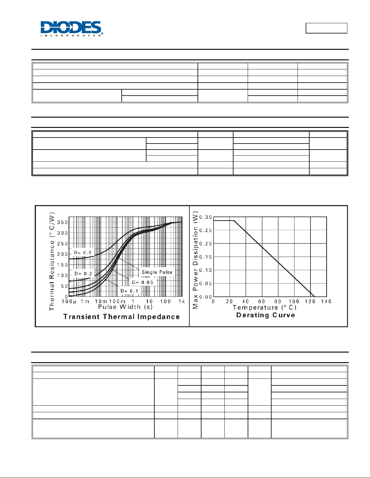
Thermal Characteristics
Characteristic Symbol Value Unit
Power Dissipation, TA = 25°C
Thermal Resistance, Junction to Ambient
Junction Temperature
Storage Temperature Range
Notes: 5. For a single device surface mounted on 25mm x 25mm x 1.6mm FR4 PCB with high coverage of 1oz copper in still air conditions.
6. As Note 5, measured at t ≤ 5 secs.
(Note 5)
(Note 6) 330
(Note 5)
(Note 6) 303
R
T
PD
θJA
T
STG
J
285
350
125 °C
-55 to +150 °C
ZHCS350
mW
Electrical Characteristics @T
= 25°C unless otherwise specified
A
Characteristic Symbol Min Typ Max Unit Test Condition
Reverse Breakdown Voltage
V
40 60 - V
R
- 300 325
Forward Voltage (Note 7)
V
F
- 335 370
- 405 460
mV
- 730 810
Reverse Current
Diode Capacitance
I
R
C
D
- 7 12
- 3.3 6 pF
Reverse Recovery Time trr - 1.6 - ns
Notes: 7. Measured under pulsed conditions. Pulse width = 300μS. Duty cycle ≤ 2%.
ZHCS350
Document number: DS33214 Rev. 3 - 2
2 of 5
www.diodes.com
IR = 100μA
I
= 30mA
F
I
= 50mA
F
I
= 100mA
F
I
= 350mA
F
μA
VR = 30V
f = 1MHz, VR = 25V
Switched from I
I
= 100mA
R
Measured @ I
= 100mA to
F
= 10mA
R
June 2012
© Diodes Incorporated
Page 3

ZHCS350
ZHCS350
Document number: DS33214 Rev. 3 - 2
3 of 5
www.diodes.com
June 2012
© Diodes Incorporated
Page 4

Package Outline Dimensions
H
C
A
B
L
SOD523
Dim Min Max
A 0.25 0.35
B 0.70 0.90
C 1.50 1.70
H 1.10 1.30
K 0.55 0.65
L 0.10 0.30
M
K
M 0.10 0.12
All Dimensions in mm
Suggested Pad Layout
X
Y
C
Dimensions Value (in mm)
Z 2.3
G 1.1
X 0.8
G
Z
Y 0.6
C 1.7
ZHCS350
ZHCS350
Document number: DS33214 Rev. 3 - 2
4 of 5
www.diodes.com
June 2012
© Diodes Incorporated
Page 5

IMPORTANT NOTICE
DIODES INCORPORATED MAKES NO WARRANTY OF ANY KIND, EXPRESS OR IMPLIED, WITH REGARDS TO THIS DOCUMENT,
INCLUDING, BUT NOT LIMITED TO, THE IMPLIED WARRANTIES OF MERCHANTABILITY AND FITNESS FOR A PARTICULAR PURPOSE
(AND THEIR EQUIVALENTS UNDER THE LAWS OF ANY JURISDICTION).
Diodes Incorporated and its subsidiaries reserve the right to make modifications, enhancements, improvements, corrections or other changes
without further notice to this document and any product described herein. Diodes Incorporated does not assume any liability arising out of the
application or use of this document or any product described herein; neither does Diodes Incorporated convey any license under its patent or
trademark rights, nor the rights of others. Any Customer or user of this document o r products described herein in such applica tions shall assume
all risks of such use and will agree to hold Diodes Incorporated and all the companies whose products are represented on Diodes Incorporated
website, harmless against all damages.
Diodes Incorporated does not warrant or accept any liability whatsoever in respect of any products purchased through unauthorized sales channel.
Should Customers purchase or use Diodes Incorporated products for any unintended or unauthorize d application, Customers shall indemnify and
hold Diodes Incorporated and its representatives harmless against all claims, damages, expenses, and attorney fees arising out of, directly or
indirectly, any claim of personal injury or death associated with such unintended or unauthorized application.
Products described herein may be covered by one or more United States, international or foreign patents pending. Product names and markings
noted herein may also be covered by one or more United States, international or foreign trademarks.
LIFE SUPPORT
Diodes Incorporated products are specifically not authorized for use as critical components in life support devices or systems without the express
written approval of the Chief Executive Officer of Diodes Incorporated. As used herein:
A. Life support devices or systems are devices or systems which:
1. are intended to implant into the body, or
2. support or sustain life and whose failure to perform when properly used in accordance with instructions for use provided in the
labeling can be reasonably expected to result in significant injury to the user.
B. A critical component is any component in a life support device or system whose failure to perform can be reasonably expected to cause the
failure of the life support device or to affect its safety or effectiveness.
Customers represent that they have all necessary expertise in the safety and regulatory ramifications of their life support devices or systems, and
acknowledge and agree that they are solely responsible for all legal, regulatory and safety-related requirements concerning their products and any
use of Diodes Incorporated products in such safety-critical, life support devices or systems, notwithstanding any devices- or systems-related
information or support that may be provided by Diodes Incorporated. Further, Customers must fully indemnify Diodes Incorporated and its
representatives against any damages arising out of the use of Diodes Incorporated products in such safety-critical, life support devices or systems.
Copyright © 2012, Diodes Incorporated
www.diodes.com
ZHCS350
ZHCS350
Document number: DS33214 Rev. 3 - 2
5 of 5
www.diodes.com
June 2012
© Diodes Incorporated
 Loading...