

Page 1
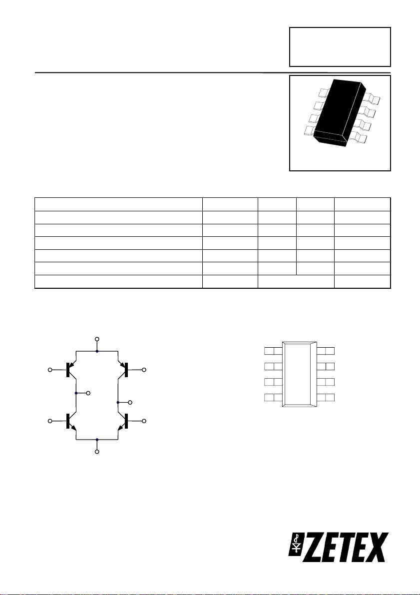
SM-8 BIPOLAR TRANSISTOR H-BRIDGE
SM-8
(8 LEAD SOT223)
PRELIMINARY DATA SHEET ISSUE B JULY 1997
FEATURES
* Compact package
* Low on state losses
* Low drive requirements
* Operates up to 40V supply
* 2 Amp continuous rating
PARTMARKING DETAIL ZHB6790
ABSOLUTE MAXIMUM RATINGS.
PARAMETER SYMBOL NPNs PNPs UNIT
Collector-Base Voltage V
Collector-Emitter Voltage V
Emitter-Base Voltage V
Peak Pulse Current I
Continuous Collector Current I
Operating and Storage Temperature Range T
CBO
CEO
EBO
CM
C
j:Tstg
50 -50 V
40 -40 V
SCHEMATIC DIAGRAM CONNECTION DIAGRAM
ZHB6790
5-5 V
6-6 A
2-2 A
-55 to +150 °C
B1
B2
Q2 Q3
E1, E4
C1, C2
E2, E3
C1,C
Q4Q1
B4
E1,E
C3,C
C3, C4
B3
B
5
2
6
4
7
4
4
8
4
B
1
3
B
2
2
E2,E
3
1
B
3
Page 2
ZHB6790
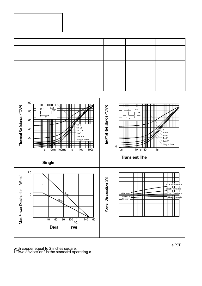
THERMAL CHARACTERISTICS
PARAMETER SYMBOL VALUE UNIT
Total Power Dissipation at T
Any single transistor on
= 25°C*
amb
Q1 and Q3 on or Q2 and Q4 on equally
Derate above 25°C*
Any single transistor on
Q1 and Q3 on or Q2 and Q4 on equally
Thermal Resistance - Junction to Ambient*
Any single transistor on
Q1 and Q3 on or Q2 and Q4 on equally
P
tot
1.25
2
10
16
100
62.5
mW/ °C
mW/ °C
°C/ W
°C/ W
W
W
100
D=t1
t1
80
60
40
20
0
100us
tP
tP
1ms 10ms 100ms 1s 10s 100s
Pulse Width
Transient Thermal Resistance
Single Transistor "On"
2.0
1.5
1.0
0.5
0
020
40 60 80 100 140120 160
T - Temperature (°C)
Derating curve
D=1
D=0.5
D=0.2
D=0.1
D=0.05
Single Pulse
60
50
40
30
20
10
0
t1
1ms100us
tP
D=t1
tP
10ms
Pulse Width
1s100ms
Transient Thermal Resistance
Q1 and Q3 or Q2 and Q4 "On"
10
Full Copper
1
Minimum
Copper
0.1
0.1
Pcb Area (inches squared)
110
Pd v Pcb Area Comparison
D=1
D=0.5
D=0.2
D=0.1
D=0.05
Single Pulse
10s
Dual Transistors
Single Transi stor
Dual Transistors
Single Transistor
100s
* The power which can be dissipated assuming the device is mounted in a typical manner on a PCB
with copper equal to 2 inches square.
"Two devices on" is the standard operating condition for the bridge. Eg. opposing NPN/PNP pairs
rurned on.
Page 3

ZHB6790
PNP TRANSISTORS
ELECTRICAL CHARACTERISTICS (at T
PARAMETER SYMBOL MIN. TYP. MAX. UNIT CONDITIONS.
Collector-Base Breakdown
Voltage
Collector-Emitter
Breakdown Voltage
Emitter-Base Breakdown
Voltage
Collector Cutoff Current I
Emitter Cutoff Current I
Collector-Emitter
Saturation Voltage
Base-Emitter
Saturation Voltage
Base-Emitter
Turn-On Voltage
Static Forward Current
Transfer Ratio
Transition Frequency f
Input Capacitance C
Output Capacitance C
Switching Times t
*Measured under pulsed conditions. Pulse width=300
V
(BR)CBO
V
(BR)CEO
V
(BR)EBO
CBO
EBO
V
CE(sat)
V
BE(sat)
V
BE(on)
h
FE
T
ibo
obo
on
t
off
= 25°C).
amb
-50 V
=-100µA
I
C
-40 V IC=-10mA*
-5 V
-0.1
-0.1
-0.14
-0.25
-0.45
-0.75
µA
µA
V
V
V
V
=-100µA
I
E
V
=-30V
CB
=-4V
V
EB
I
=-100mA, IB=-0.5mA*
C
=-500mA, IB=-5mA*
I
C
I
=-1A, IB=-10mA*
C
=-2A, IB=-50mA*
I
C
-1.0 V IC=-1A, IB=-10mA*
-0.75 V IC=-1A, VCE=-2V*
300
200
150
I
=-100mA, VCE=-2V
C
=-1A, VCE=-2V*
I
C
I
=-2A, VCE=-2V*
C
100 MHz IC=-50mA, VCE=-5V
f=50MHz
225 pF VEB=-0.5V, f=1MHz
24 pF VCB=-10V, f=1MHz
35
600
µs. Duty cycle ≤ 2%.
ns IC=-500mA,
I
= -50mA
B1
=-50mA, VCC=-10V
I
B2
Page 4

ZHB6790
NPN TRANSISTORS
ELECTRICAL CHARACTERISTICS (at T
PARAMETER SYMBOL MIN. TYP. MAX. UNIT CONDITIONS.
Collector-Base Breakdown
Voltage
Collector-Emitter
Breakdown Voltage
Emitter-Base Breakdown
Voltage
Collector Cutoff Current I
Emitter Cutoff Current I
Collector-Emitter
Saturation Voltage
Base-Emitter
Saturation Voltage
Base-Emitter
Turn-On Voltage
Static Forward Current
Transfer Ratio
Transition Frequency f
Input Capacitance C
Output Capacitance C
Switching Times t
*Measured under pulsed conditions. Pulse width=300
V
(BR)CBO
V
(BR)CEO
V
(BR)EBO
CBO
EBO
V
CE(sat)
V
BE(sat)
V
BE(on)
h
FE
T
ibo
obo
on
t
off
= 25°C).
amb
50 V
=100µA
I
C
40 V IC=10mA*
5V
0.1
µA
0.1
µA
V
0.1
V
0.16
V
0.5
V
0.35
=100µA
I
E
V
=35V
CB
=4V
V
EB
I
=100mA, IB=0.5mA*
C
=500mA, IB=2.5mA*
I
C
I
=1A, IB=5mA*
C
=2A, IB=30mA*
I
C
0.9 V IC=1A, IB=10mA*
0.73 V IC=1A, VCE=2V*
500
400
150
I
=100mA, VCE=2V*
C
=1A, VCE=2V*
I
C
I
=2A, VCE=2V*
C
150 MHz IC=50mA, VCE=5V
f=50MHz
200 pF VEB=0.5V, f=1MHz
16 pF VCB=10V, f=1MHz
33
1300
µs. Duty cycle ≤ 2%.
ns IC=500mA, IB!=50mA
I
=50mA, VCC=10V
B2
Page 5

PNP TRANSISTOR
TYPICAL CHARACTERISTICS
ZHB6790
olts)
(V
-
V
in
alised Ga
Norm
-
h
1.8
1.6
1.4
1.2
1.0
0.8
0.6
0.4
0.2
0
IC/IB=100
IC/IB=40
IC/IB=10
0.01 0.1 1 10
T
=25°C
amb
IC- Collector Current (Amps)
CE(sat)
V
1.6
1.4
1.2
1.0
0.8
0.6
0.4
0.2
0
+100°C
+25°C
-55°C
0.01 0.1
IC-
Collector Current (Amps)
v IC
1
VCE=2V
750
n
Gai
500
cal
ypi
T
-
250
h
10
hFEv IC V
1.8
1.6
1.4
1.2
ts)
ol
V
1.0
(
-
0.8
0.6
V
0.4
0.2
0
-55°C
+25°C
+100°C
0.01 0.1 1 10
IC/IB=100
IC- Collector Current (Amps)
CE(sat)
V
1.6
1.4
1.2
ts)
1.0
- (Vol
0.8
0.6
0.4
V
0.2
0
+100°C
0.01 0.1 1 10
IC-
Collector Current (Amps)
-55°C
+25°C
BE(sat)
v IC
IC/IB=100
v IC
-55°C
1.6
1.4
1.2
ts)
ol
1.0
V
(
-
0.8
0.6
V
0.4
0.2
0
0
+25°C
+100°C
0.01 0.1 1 10
IC-
Collector Current (Amps)
BE(on)
V
v IC
VCE=2V
Page 6

NPN TRANSISTOR
TYPICAL CHARACTERISTICS
ZHB6790
olts)
(V
-
V
n
i
alised Ga
Norm
-
h
T
=25°C
0.8
0.6
0.4
0.2
0
IC/IB=200
IC/IB=100
IC/IB=10
0.01 0.1 1 10
amb
0.8
ts)
0.6
ol
V
(
-
0.4
V
0.2
0
IC- Collector Current (Amps)
CE(sat)
V
1.6
1.4
1.2
1.0
0.8
0.6
0.4
0.2
0
0
+100°C
+25°C
-55°C
0.01 0.1
IC-
Collector Current (Amps)
v IC
VCE=2V
1.5K
n
1K
Gai
cal
ypi
T
500
-
h
10
1
olts)
(V
-
V
1.6
1.4
1.2
1.0
0.8
0.6
0.4
0.2
0
hFEv IC V
-55°C
+25°C
+100°C
0.01 0.1 1 10
IC/IB=100
IC- Collector Current (Amps)
CE(sat)
V
+100°C
0.01 0.1 1 10
IC-
Collector Current (Amps)
-55°C
+25°C
BE(sat)
v IC
v IC
IC/IB=100
olts)
V
(
-
-55°C
1.6
1.4
1.2
1.0
0.8
V
0.6
0.4
0.2
0
0
+25°C
+100°C
0.01 0.1 1 10
VCE=2V
IC- Collector Current (Amps)
BE(on)
V
v IC
Page 7

SAFE OPERATING AREA
ZHB6790
10
1
DC
100m
10m
100m 100
1s
100ms
10ms
1ms
100µs
110
VCE - Collector Emitter Voltage (V)
Safe Operating Area (Full Copper)
Note: The Safe Operating Area (SOA) charts shown are a combination of the worst case secondary
breakdown characteristics for the NPN/PNP pair, and the thermal curves demonstrating the
power dissipation capability of the energised ZHB part (opposing NPN-PNP switched on) when
mounted on a 50mm x 50mm FR4 PCB. The two cases show:
i) full copper present and
ii) with minimal copper present - this being defined as an SM-8 footprint with 1.5mm tracks to
see note below
10
1
DC
100m
10m
100m 100
1s
100ms
10ms
1ms
100µs
110
VCE - Collector Emitter Voltage (V)
Safe Operating Area (Minimum Copper)
see note below
the edge of the PCB.
For example, on a 50mm x 50mm full copper PCB, the ZHB6790 will safely dissipate 2W under
DC conditions, taking note of continuous current ratings and voltage limits. Higher powers can
be tolerated for pulsed operation, while the shorter pulse widths (100µs and 1ms) being relevant
for assessment of switching conditions.
The ZHB6790 H-Bridge can be modelled within SPICE using the following transistor models
configured in the standard H-Bridge topology, as shown in the schematic diagram of this datasheet.
ZETEX H Bridge NPN transistors Spice model Last revision 4/7/97
.MODEL H6790N NPN IS =2.505E-12 NF =1.0058 BF =1360 IKF=1.3 VAF=35
+ISE=.24E-12 NE =1.38 NR =1.001 BR =125 IKR=1 VAR=8 ISC=.435E-12
+NC =1.213 RB =.2 RE =.043 RC =.04 CJC=54.3E-12 MJC=.475 VJC=.765
+CJE=247E-12 TF =.851E-9 TR =15.7E-9
*
*
*ZETEX H Bridge PNP transistors Spice model Last revision 4/7/97
.MODEL H6790P PNP IS=1.09684E-12 NF=1.0102 BF=650 IKF=1.7 VAF=23.5
+ISE=9.88593E-14 NE=1.47256 NR=1.00391 BR=270 IKR=0.2 VAR=30
+ISC=5.4933E-14 NC=1.07427 RB=0.055 RE=0.049 RC=0.078 CJC=96E-12
+MJC=0.495 VJC=0.67 CJE=275E-12 TF=0.75E-9 TR=10.8E-9
*
(C) 1997 ZETEX PLC
The copyright in these models and the design embodied belong to Zetex PLC (Zetex). They are supplied
free of charge by Zetex for the purpose of research and design and may be used or copied intact (including
this notice) for that purpose only. All other rights are reserved. The models are believed accurate but no
condition or warranty as to their merchantability or fitness for purpose is given and no liability in respect of
any use is accepted by Zetex PLC, its distributors or agents. Zetex PLC, Fields New Road, Chadderton,
Page 8

D
ZHB6790
He
E
5
b
o
6
7
8
4
3
e2
2
1
e1
A
A1
45°
c
Lp
3
Dim Millimetres Inches
Min Typ Max Min Typ Max
A 1.7 0.067
A1 0.02 0.1 0.0008 0. 004
b 0.7 0.028
c 0.24 0.32 0.009 0.013
D 6.3 6.7 0.248 0.264
E 3.3 3.7 0.130 0.145
e1 4.59 0.180
e2 1.53 0.060
He 6.7 7.3 0.264 0.287
Lp 0.9 0.035
Zetex plc.
Fields New Road, Chadderton, Oldham, OL9-8NP, United Kingdom.
Telephone: (44)161 622 4422 (Sales), (44)161 622 4444 (General Enquiries)
Fax: (44)161 622 4420
Zetex GmbH Zetex Inc. Zetex (Asia) Ltd. These are supported by
Streitfeldstraße 19 47 Mall Drive, Unit 4 3510 Metroplaza, Tower 2 agents and distributors in
D-81673 München Commack NY 11725 Hing Fong Road, major countries world-wide
Germany USA Kwai Fong, Hong Kong
Telefon: (49) 89 45 49 49 0 Telephone: (516) 543-7100 Telephone:(852) 26100 611 Internet:
Fax: (49) 89 45 49 49 49 Fax: (516) 864-7630 Fax: (852) 24250 494 http://www.zetex.com
This publication is issued to provide outline information only which (unless agreed by the Company in writing) may not be used, applied
or reproduced for any purpose or form part of any order or contract or be regarded as a representation relating to the products or
services concerned. The Company reserves the right to alter without notice the specification, design, price or conditions of supply of any
product or service.
Zetex plc 1997
 Loading...