

Page 1
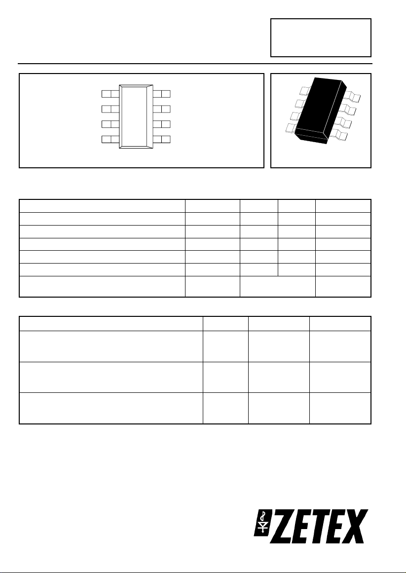
SM-8 COMPLEMENTARY MEDIUM POWER
SM-8
(8 LEAD SOT223)
DARLINGTON TRANSISTORS
ISSUE 2 February 1997
ZDT6702
C
1
C
1
C
2
C
2
B
1
NPN
E
1
B
2
PNP
E
2
PARTMARKING DETAIL T6702
ABSOLUTE MAXIMUM RATINGS.
PARAMETER SYMBOL NPN PNP UNIT
Collector-Base Voltage V
Collector-Emitter Voltage V
Emitter-Base Voltage V
Peak Pulse Current I
Continuous Collector Current I
Operating and Storage Temperature
Range
CM
C
T
CBO
CEO
EBO
j:Tstg
80 -80 V
60 -60 V
10 -10 V
4-4 A
1.75 -1.75 A
-55 to +150 °C
THERMAL CHARACTERISTICS
PARAMETER SYMBOL VALUE UNIT
Total Power Dissipation at T
Any single die on
= 25°C*
amb
Both die on equally
Derate above 25°C*
Any single die on
Both die on equally
Thermal Resistance - Junction to Ambient*
Any single die on
Both die on equally
* The power which can be dissipated assuming the device is mounted in a typical manner
on a PCB with copper equal to 2 inches square.
P
tot
2.25
2.75
18
22
55.6
45.5
W
W
mW/ °C
mW/ °C
°C/ W
°C/ W
Page 2
ZDT6702
NPN TRANSISTOR
ELECTRICAL CHARACTERISTICS (at T
PARAMETER SYMBOL MIN. TYP. MAX. UNIT CONDITIONS.
= 25°C unless otherwise stated).
amb
Collector-Base
Breakdown Voltage
Collector-Emitter
Breakdown Voltage
Emitter-Base
Breakdown Voltage
Collector Cutoff
Current
Emitter Cutoff Current I
Colllector-Emitter
Cutoff Current
Collector-Emitter
Saturation Voltage
Base-Emitter
Saturation Voltage
Base-Emitter
Turn-On Voltage
Static Forward
Current Transfer Ratio
Transition Frequency f
V
(BR)CBO
V
(BR)CEO
V
(BR)EBO
I
CBO
EBO
I
CES
V
CE(sat)
V
BE(sat)
V
BE(on)
h
FE
T
80 200 V
=100µA
I
C
60 100 V IC=10mA*
10 15 V
0.5 10
10
nA
µA
=100µA
I
E
=60V
V
CB
V
=60V,T
CB
0.1 10 nA VEB=8V
50 500 nA V
0.83
1.0
0.95
1.28VV
=60V
CE
IC=0.5A, IB=0.5mA*
I
=1.75A, IB=2mA*
C
1.68 1.85 V IC=1.75A, IB=2mA*
1.55 1.75 V IC=1.75A, VCE=5V*
5K
5K
3.5K
0.5K
13K
13K
9K
2K
I
=10mA, VCE=5V
C
=500mA, VCE=5V
I
C
I
=2A, VCE=5V
C
=4A, VCE=5V*
I
C
140 MHz IC=100mA, VCE=10V
f=100MHz
amb
=100°C
Input Capacitance C
Output Capacitance C
Switching Times t
ibo
obo
on
t
off
70 pF VEB=500mV, f=1MHz
15 pF VCB=10V, f=1MHz
0.5
2.1
*Measured under pulsed conditions. Pulse width=300
µs
µs
µs. Duty cycle ≤ 2%
=500mA, VCE=10V
I
C
I
=0.5mA
B1=IB2
Page 3
ZDT6702
PNP TRANSISTOR
ELECTRICAL CHARACTERISTICS (at T
PARAMETER SYMBOL MIN. TYP. MAX. UNIT CONDITIONS.
Collector-Base
Breakdown Voltage
Collector-Emitter
Breakdown Voltage
Emitter-Base
Breakdown Voltage
Collector Cutoff
Current
Emitter Cutoff Current I
Collector-Emitter
Cutoff Current
Collector-Emitter
Saturation Voltage
Base-Emitter
Saturation Voltage
Base-Emitter Turn-On
Voltage
Static Forward
Current Transfer Ratio
Transition Frequency f
V
(BR)CBO
V
CEO(SUS)
V
(BR)EBO
I
CBO
EBO
I
CES
V
CE(sat)
V
BE(sat)
V
BE(on)
h
FE
T
-80 -120 V
-60 -90 V IC=-10mA*
-10 -15 V
2K
2K
1.5K
1K
= 25°C unless otherwise stated).
amb
=-100µA
I
C
=-100µA
I
E
-0.5 -10
-10
nA
µA
V
CB
V
CB
=-60V
=-60V, T
-0.1 -10 nA VEB=-8V
-50 -500 nA V
-0.86
-1.05
-1.0
-1.28VV
=-60V
CE
IC=-0.5A, IB=-0.5mA*
I
=-1.75A, IB=-2mA*
C
-1.7 -1.9 V IC=-1.75A, IB=-2mA*
-1.55 -1.85 V IC=-1.75A, VCE=-5V*
8K
8K
7K
4K
I
=-10mA, VCE=-5V*
C
=-500mA, VCE=-5V*
I
C
I
=-2A, VCE=-5V*
C
=-4A, VCE=-5V*
I
C
140 MHz IC=-100mA, VCE=-10V
f=100MHz
amb
=100°C
Input Capacitance C
Output Capacitance C
Switching Times t
ibo
obo
on
t
off
90 pF VEB=-0.5V, f=1MHz
25 pF VCE=-10V, f=1MHz
0.75
1.2
*Measured under pulsed conditions. Pulse width=300
µs
µs
s. Duty cycle ≤ 2%
µ
I
=-0.5A, VCE=-10V
C
I
=-0.5mA
B1=IB2
Page 4

ZDT6702
TYPICAL CHARACTERISTICS (NPN TRANSISTOR)
1.2
+25°C
1.0
0.8
0.6
0.4
0.2
0
1m
10m 100m 1 10
IC/IB=1000
IC/IB=500
IC- Collector Current (A)
VCE(sat) v IC
IC/IB=1000
1.0
0.8
0.6
0.4
0.2
1m 10m 100m 1 10
IC- Collector Current (A)
VCE(sat) v IC
-55°C
+25°C
+85°C
+150°C
20K
VCE=5V
16K
12K
8K
4K
0
IC- Collector Current (A)
hFE v IC
2.0
VCE=5V
1.6
1.2
0.8
0.4
0
1m 10m 100m 1 10
IC- Collector Current (A)
VBE(on) v IC
+85°C
+25°C
-55°C
-55°C
+25°C
+85°C
+150°C
2.0
IC/IB=1000
1.6
1.2
0.8
0.4
0
IC- Collector Current (A)
VBE(sat) v IC
10
1
100m
10m
100m
DC
1s
100ms
10ms
1ms
100us
VCE- Collector Emitter Voltage (V)
1 10 100
Safe Operati ng Area
100m1m 10m 100m 1 10 10m1m 101
-55°C
+25°C
+85°C
+150°C
Page 5

ZDT6702
TYPICAL CHARACTERISTICS (PNP TRANSISTOR)
1.2
IC/IB=1000
1.0
0.8
0.6
0.4
0.2
0
1m 10m 100m 1 10
IC- Collector Current (A)
V
CE(sat)
2.0
IC/IB=1000
1.6
1.2
0.8
0.4
20k
15k
10k
+25°C
1.0
0.8
0.6
0.4
0.2
0
1m
10m 100m 1 10
IC- Collector Current (A)
V
VCE=5V
5k
CE(sat)
v I
IC/IB=1000
IC/IB=500
C
+85°C
+25°C
-55°C
v I
-55°C
+25°C
+85° C
+150° C
C
-55° C
+25°C
+85°C
+150°C
0
1m 10m 100m 1 10 1m 10m 100m 101
IC- Collector Current (A)
hFEv I
C
2.0
VCE=5V
1.6
1.2
0.8
0.4
0
1m 10m 100m 1 10 100m
-55° C
+25° C
+85° C
+150° C
IC - Collector Current (A)
V
v I
BE(on)
C
0
IC- Collector Current (A)
V
BE(sat)
10
1
DC
100m
10m
1s
100ms
10ms
1ms
100us
110100
VCE- Collector Emitter Voltage (V)
Safe Operating Area
v I
C
Page 6

ZDT6702
OTHER CHARACTERISTICS
D= 1
50
40
30
20
10
0
100us
D= t1
t1
tP
tP
1ms 10ms 100ms 1s 10s 100s
Pulse Width
Transient Thermal Resistance
(single devic e)
2.00
1.50
1.00
Rs = 1M ohm
Rs = o/ c
0.50
0
10
VCE - Collector Emitter Voltage (V )
Voltage Derating
D= 0. 5
D= 0. 2
D= 0. 1
D= 0. 05
Single Pulse
100
4
3
2
1
0
0
20 40 60 80 100 120 140 160
T - Ambient Temperature (° C)
Derating curve
(single devic e)
2.00
1.50
1.00
Rs = o/ c
0.50
0
10
VCE - Collector Emitter Voltage (V )
Voltage Derating
100
Page 7

ZDT6702
He
E
5
b
D
3
6
7
8
o
45°
4
3
e2
2
1
Lp
e1
c
A
A1
Dim Millimetres Inches
Min Typ Max Min Typ Max
A 1.7 0.067
A1 0.02 0.1 0.0008 0.004
b 0.7 0.028
c 0.24 0.32 0.009 0.013
D 6.3 6.7 0.248 0.264
E 3.3 3.7 0.130 0.145
e1 4.59 0.180
e2 1.53 0.060
He 6.7 7.3 0.264 0.287
Lp 0.9 0.035
15° 15°
α
10° 10°
β
Zetex plc.
Fields New Road, Chadderton, Oldham, OL9-8NP, United Kingdom.
Telephone: (44)161 622 4422 (Sales), (44)161 622 4444 (General Enquiries)
Fax: (44)161 622 4420
Zetex GmbH Zetex Inc. Zetex (Asia) Ltd. These are supported by
Streitfeldstraße 19 47 Mall Drive, Unit 4 3510 Metroplaza, Tower 2 agents and distributors in
D-81673 München Commack NY 11725 Hing Fong Road, major countries world-wide
Germany USA Kwai Fong, Hong Kong
Telefon: (49) 89 45 49 49 0 Telephone: (516) 543-7100 Telephone:(852) 26100 611 Internet:
Fax: (49) 89 45 49 49 49 Fax: (516) 864-7630 Fax: (852) 24250 494 http://www.zetex.com
This publication is issued to provide outline information only which (unless agreed by the Company in writing) may not be used, applied
or reproduced for any purpose or form part of any order or contract or be regarded as a representation relating to the products or
services concerned. The Company reserves the right to alter without notice the specification, design, price or conditions of supply of
any product or service.
Zetex plc 1997
 Loading...