

Page 1
A
Product Line o
f
Diodes Incorporated
ZABG6002
LOW POWER 6 STAGE FET LNA AND MIXER BIAS CONTROLLER
Summary
The ZABG6002 is a programmable low power depletion mode FET bias and mixer controller intended primarily for
satellite Low Noise Blocks (LNBs). Designed to provide system flexibility the ZABG6002 can be programmed to bias
six low noise amplifier (LNA) stages or four LNA and two active mixer stages, allowing the ZABG6002 to be used in
several system designs.
Combining advanced IC process and packaging techniques, the ZABG6002 operates with minimal current over a
wide supply voltage. The small package and reduced component count minimizes the PCB area whilst enhancing
overall LNB reliability.
Features
• Six stage FET bias controller, two configurable as
mixer stages
• Operating range of 3.0V to 8.0V
• Amplifier FET drain voltages set at 2.0V, mixer
drain voltage set at 0.25V
• Amplifier FET drain current selectable from 0 to
15mA, mixer current from 0 to 7.5mA
• Switchable FET’s for power management
• FET drain voltages and currents held stable over
temperature and V
variations
CC
• FETs protected against overstress during powerup and power-down.
• Internal negative supply generator allowing single
supply operation (available for external use)
• Low quiescent supply current, 1.6mA typical
• Low external component count
Applications
• Twin LNB’s
• Quad LNB’s
• US LNB’s
• Microwave links
• PMR and Cellular telephone systems
Pin Assignments
1
1
G2
G2
G2
D3
D3
D3
G3
G3
G3
1
G
G
G
d
d
d
n
n
n
G
G
G
D1
D1
D1
Cnb1
Cnb1
Cnb1
D1
D1
G1
G1
D2
D2
G2
G2
D3
D3
G3
G3
RcalM
RcalM
Gnd
Gnd
Cnb1
Cnb1
Vcc
Vcc
Vcc
Cnb2
Cnb2
Cnb2
1
1
QFN2044
4
4
4
D
D
D
G4
G4
G4
D5D2
D5D2
D5D2
G5
G5
G5
D6
D6
D6
G6
G6
G6
Rcal1RcalM
Rcal1RcalM
Rcal1RcalM
ub
ub
ub
s
s
s
C
Rcal2
C
Rcal2
C
Rcal2
QSOP20
CsubCsubCsub
Vcc
Vcc
D4
D4
G4
G4
D5
D5
G5
G5
D6
D6
G6
G6
Rcal1
Rcal1
Rcal2
Rcal2
CsubCnb2
CsubCnb2
Twin LNB System Diagrams
Vertical
Vertical
ZXHF
ZABG
ZABG
6002
6002
Horizontal
Horizontal
ZABG6002
Document number: DS32078 Rev. 1 - 2
ZXHF
5002
5002
www.diodes.com
1 of 12
Left
Left
Right
Right
ZABG
ZABG
6002
6002
2x2 MUX
2x2 MUX
© Diodes Incorporated
ZLNB
ZLNB
102
102
May 2010
Page 2

A
Product Line o
f
Diodes Incorporated
ZABG6002
Device Description
The ZABG series of devices are designed to meet the bias requirements of GaAs and HEMT FETs commonly used
in satellite receiver LNBs with a minimum of external components whilst operating from a minimal voltage supply
and using minimal current.
The ZABG6002 has six FET bias stages that can be user programmed to provide either a two plus four
arrangement of amplifier FET stages or a two plus two arrangement of amplifier FET stages along with two active
mixer FET stages. Programming of the FET bias stage arrangement and the operating currents of each FET group
is achieved by resistors connected to the Rcal1, Rcal2 and RcalM pins, allowing input FETs to be biased for
optimum noise, amplifier FETs for optimum gain and mixer FETs (if used) for optimum conversion gain. Amplifier
FETs can be operated at currents in the range 0 to 15mA and mixer FETs in the range 0.5 to 7.5mA.
Drain voltages of amplifier stages are set at 2.0V and mixer stages at 0.3V. The drain supplies are current limited to
approximately 5% above the operating currents set by their associated Rcal resistors.
As an additional feature the Rcal pins can also be used as logic inputs to disable pairs of FETs as part of a power
management scheme or simply an alternative to LNA switching. Driven to a logic high (>3.0V), the inputs disable
their associated FET bias stages by switching gate feeds to -2.5V and drain feeds open circuit.
Depletion mode FETs require a negative voltage bias supply when operated in grounded source circuits. The
ZABG6002 includes an integrated low noise switched capacitor DC-DC converter generating a regulated output of -
2.5V to allow single supply operation. To aid efficiency and 3.3V systems the ZABG6002 has been design to used
with supply rails of 3.3V to 8V
It is possible to use less than the devices full complement of FET bias controls, unused drain and gate connections
can be left open circuit without affecting operation of the remaining bias circuits.
To protect the external FETs the circuits have been designed to ensure that, under any conditions including power
up/down transients, the gate drive from the bias circuits cannot exceed -3V. Additionally each stage has its own
individual current limiter. Furthermore if the negative rail experiences a fault condition, such as overload or short
circuit, the drain supply to the FETs will shut down avoiding excessive current flow.
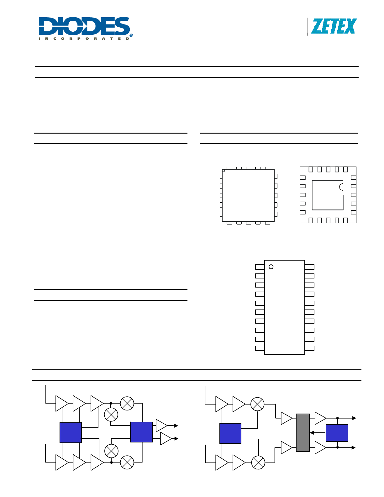
The ZABG6002 is available in the 20 pin 4mm x 4mm QFN or QSOP20 package.
Device operating temperature is -40°C to 85°C to suit a wide range of environmental conditions.
ZABG6002
Document number: DS32078 Rev. 1 - 2
2 of 12
www.diodes.com
May 2010
© Diodes Incorporated
Page 3
A
f
Maximum Ratings
Parameter Rating Unit
Supply Voltage -0.6 to +10 V
Supply Current 100 mA
Power Dissipation 600 mW
Operating Temperature Range -40 to +85 °C
Storage Temperature Range -40 to 150 °C
Product Line o
Diodes Incorporated
ZABG6002
Electrical Characteristics Measured at T
R
= 68K (setting I
CALM
to 5mA) unless otherwise stated
D3/6
= 25°C, VCC = 3.3V (Note 1), R
AMB
CAL1
= R
CAL2
= 36K (setting I
D1/2/4/5
to 10mA),
Parameter Conditions Symbol Min. Typ. Max. Unit
Operating Voltage Range VCC 3.0 8.0 V
I
= 0 ICC 1.6 4.0 mA
Supply Current
Substrate Voltage
Oscillator Frequency F
D1-6
I
= 10mA, no R
D1-6
I
= 0 V
CSUB
I
= -200uA V
CSUB
CALM
I
CC(L)
CSUB
CSUB(L)
OSC
62 64 mA
-3.0 -2.65 -2.0 V
-2.55 -2.0 V
150 260 600 kHz
Gate Characteristics
Gate (G1 to G6, resistor R
not present)
CALM
Current Range IG -100 +500 uA
Voltage Low ID = 12mA, IG = -10uA V
Voltage High ID = 8mA, IG = 0 V
I
Voltage Disabled
(*1)
= 0, IG = -10uA,
D
RCAL1-2
= 3.0V
V
-3.0 -2.5 -2.0 V
G(L)
0 0.7 1.0 V
G(H)
V
-3.0 -2.5 -2.0 V
G(DIS)
Gate (G3 and G6, resistor R
CALM
present)
Current Range IG -100 +500 uA
Voltage Low ID = 6mA, IG = -10uA V
Voltage High ID = 4mA, IG = 0 V
I
Voltage Disabled
(*1)
= 0, IG = -10uA,
D
= V
V
RCAL2
RCALM
3.0V
-3.0 -2.5 -2.0 V
G(L)
0 0.7 1.0 V
G(H)
V
-3.0 -2.5 -2.0 V
G(DIS)
Drain Characteristics
Drain (D1 to D6, resistor R
M not present)
CAL
Current Range ID 0 15 mA
Current Operating
Current Disabled
(*1)
V
Voltage Operating ID = 10mA V
Standard Application
Circuit
= 0, V
D
= 3.0V I
RCAL
I
8 10 12 mA
D(OP)
10 uA
D(DIS)
1.8 2.0 2.2 V
D(OP)
ZABG6002
Document number: DS32078 Rev. 1 - 2
3 of 12
www.diodes.com
May 2010
© Diodes Incorporated
Page 4
A
Product Line o
f
Diodes Incorporated
ZABG6002
Electrical Characteristics (Cont.) Measured at T
10mA), R
= 68K (setting I
CALM
to 5mA) unless otherwise stated
D3/6
= 25°C, VCC = 3.3V (Note 1), R
AMB
CAL1
= R
CAL2
= 36K (setting I
D1/2/4/5
to
Parameter Conditions Symbol Min. Typ. Max. Unit
Drain Characteristics
Drain (D3 and D6, resistor R
M present)
CAL
Current Range IDM 0.5 7.5 mA
Current Operating
Current Disabled
(*1)
Voltage Operating ID = 5mA V
Standard Application
Circuit
V
R
D
CALM
= 0, V
not present
RCAL
= 3.0V,
I
4 5 6 mA
DM(OP)
I
10 uA
DM(DIS)
0.25 0.3 0.35 V
DM(OP)
R
(1 and 2)
CAL
Disable Threshold
Input Current V
(*1)
V
= 3.0V I
RCAL
RCAL(DIS)
RCAL(DIS)
1.8 2.7 3.0 V
1.7 10 uA
R
CALM
Disable Threshold
R
Range R
CALM
(*1)
R
CALM(DIS)
CALM
1.5M 3.3M 5.0M
39k 390k
Ω
Ω
Voltage and Temperature dependence (R
delta ID vs VCC V
delta ID vs TOP T
delta VD vs VCC V
delta VD vs TOP T
M not present)
CAL
= 3.3 to 8.0V dID/dVCC 1.2 %/V
CC
= -40°C to +85°C dID/dTOP 0.05 %/°C
OP
= 3.3 to 8.0V dVD/dVCC 0.05 %/V
CC
= -40°C to +85°C dVD/dTOP 50 ppm/°C
OP
Output Noise
C
Drain Voltage
Gate Voltage
Notes: 1. To disable FET stages 3 and 6, pin R
further information.
2. The characteristics are measured using up to three external reference resistors, R
Resistor R
is present, resistor R
3. The negative bias voltages are generated on-chip using an internal oscillator. Two external capacitors, C
this purpose.
4. The QFN2044 exposed pad must either be connected to Csub or left open circuit.
5. Noise voltage measurements are made with FETs and gate and drain capacitors of value 10nF in place. Noise voltages are not measured in production.
6. ESD sensitive, handling precautions are recommended.
sets the drain current of FETs 1 and 4. If R
CAL1
sets the drain currents of FETs 2 and 5 and R
CAL2
GATE-GND
C
DRAIN-GND
C
GATE-GND
C
DRAIN-GND
must be set to 3V or above and pin R
CAL2
ZABG6002
Document number: DS32078 Rev. 1 - 2
= 10nF,
= 10nF
= 10nF,
= 10nF
is not present, resistor R
CALM
www.diodes.com
sets the drain currents of FETs 3 and 6.
CALM
4 of 12
V
V
should be open circuit. See applications section for
CALM
, R
CAL1
0.02 Vpk-pk
D(NOISE)
0.005 Vpk-pk
G(NOISE)
and R
CAL2
sets the drain currents of FETs 2, 3, 5 and 6. If R
CAL2
, wired from pins R
CALM
and C
NB
CAL1/2/M
of value 47nF are required for
SUB
to ground.
© Diodes Incorporated
CALM
May 2010
Page 5

A
Product Line o
f
Diodes Incorporated
ZABG6002
Typical Characteristics Measured at T
I
to 5mA) unless otherwise stated
D3/6
ZABG 6002 Drain Voltage (D1 - D6) vs Temperature
2.3
2.2
2.1
2
Drain Volt age (V)
1.9
1.8
1.7
-40 -20 0 20 40 60 80
ZABG 6002 Drain Voltage (D3 & D6 onl y) vs Temperature
0.5
0.4
0.3
Temperature ( ° C)
= 25°C, VCC = 3.3V, R
AMB
= R
CAL1
= 36K (setting ID to 10mA), R
CAL2
ZABG 6002 Drain Current (D1 - D6) vs Temperature
20
18
16
14
12
10
8
Drain Cu r r en t (mA)
6
4
2
0
-40-200 20406080
ZABG6002 Drain Current (D3 & D6 only) vs Temperature
10
8
6
Temperature ( ° C)
CALM
= 68K (setting
0.2
Drain Voltage (V)
0.1
0
-40 -20 0 20 40 60 80
ZAB G6002 Substrate Vo ltage vs Substrate Current
-2
-2.2
-2.4
-2.6
Substrate Voltage (V)
-2.8
-3
0 50 100 150 200 250
Temperature ( ° C)
Substrate Current (uA)
4
Drain Cur r e nt (mA)
2
0
-40-200 20406080
Temperature (° C)
ZABG6002
Document number: DS32078 Rev. 1 - 2
5 of 12
www.diodes.com
May 2010
© Diodes Incorporated
Page 6

A
Product Line o
f
Diodes Incorporated
ZABG6002
Typical Characteristics (Cont.) Measured at T
(setting I
to 5mA) unless otherwise stated
D3/6
ZA BG6002 Drain Voltage vs Drai n Current (D1-D6)
2.2
2.1
2
Drain Voltage (V)
1.9
1.8
051015
ZABG6002 Drain Voltage vs Drain Current ( D 3 & D6 only)
0.5
0.4
0.3
0.2
Drain Voltage ( V)
0.1
Drain Current (mA)
= 25°C, VCC = 3.3V, R
AMB
= R
CAL1
15
10
5
Drain Current (m A)
0
10 100 1000
10
5
Drain Cu rrent (mA)
= 36K (setting ID to 10mA), R
CAL2
ZABG 6002 Drain Current vs R
R
(k)
CAL
ZABG6002 Drain Current vs R
CALM
CAL
CALM
= 68K
0
0510
Drain Current (mA)
0
10 100 1000
R
(k)
CAL
ZABG6002
Document number: DS32078 Rev. 1 - 2
6 of 12
www.diodes.com
May 2010
© Diodes Incorporated
Page 7

A
Product Line o
f
Diodes Incorporated
ZABG6002
Application Information
The ZABG6002 is a flexible device and can be set up in a number of ways.
1. 6 LNA stages to provide standard bias to the GaAs or HEMT FET’s
2. 4 LNA stages to provide standard bias to the GaAs or HEMT FET’s plus 2 active mixer stages
3. Power down FET groups for LNA switching or power saving.
The truth table below shows the function of these features.
R
Pin Resistor Termination
cal
Rcal1 Rcal2 RcalM Bias 1 Bias 4 Bias 2 Bias 5 Bias 3 Bias 6
Gnd Gnd Open On On On On On On
Gnd Gnd Gnd On On On On Mixer Mixer
Gnd 3V Open On On Off Off Off Off
Gnd 3V Gnd On On Off Off Mixer Mixer
3V Gnd Open Off Off On On On On
3V Gnd Gnd Off Off On On Mixer Mixer
3V 3V Open Off Off Off Off Off Off
3V 3V Gnd Off Off Off Off Mixer Mixer
ZABG6002 in 6 LNA mode
Below is a partial applications circuit for the ZABG6002 showing all external components needed for biasing one of
the six FET stages available as a normal LNA bias. Each bias stage is provided with a gate and drain pin. The drain
pin provides a regulated 2.0V supply that includes a drain current monitor. The drain current taken by the external
FET is compared with a user selected level, generating a signal that adjusts the gate voltage of the FET to obtain
the required drain current. If for any reason, an attempt is made to draw more than the user set drain current from
the drain pin, the drain voltage will be reduced to ensure excess current is not taken. The gate pin drivers are also
current limited.
The bias stages are split up into two groups, with the drain current of each group set by an external R
R
CAL
ZABG6002
Document number: DS32078 Rev. 1 - 2
JF2
JF2
* Stripline Elements
* Stripline Elements
1 sets the drain currents of stages 1 and 4, whilst R
FET Stage
L*
L*
C* C1
C* C1
L*
L*
C*
C*
10nF
10nF
C2
C2
10nF
10nF
1st LNA
Stages
D2
D2
G2
G2
D3
D3
G3
RcalM
RcalM
47nF
47nF
47nF
CAL
7 of 12
www.diodes.com
2nd LNA
Stages
CNB
CNB
CNB
G1
G1
Gnd
Gnd
Vcc
D1
Vcc
D1
ZABG6002
ZABG6002
Cnb1
Cnb1
Cnb2
Cnb2
CSUB
CSUB
47nF
47nF
2 sets the drain currents of stages 2,3,5 and 6.
D4
D4
Csub
Csub
3rd LNA/Mixer
G4
G4
D5
D5
G5
G5
D6
D6
G6
G6
Rcal1
Rcal1
Rcal2
Rcal2
RCAL2
RCAL2
36k
Stages
RCAL1
RCAL1
36k
Vcc
Vcc
resistor.
CAL
May 2010
© Diodes Incorporated
Page 8

A
Product Line o
f
Diodes Incorporated
ZABG6002
This allows the optimization of drain currents for differing tasks such as input stages where noise can be critical and
later amplifier stages where gain may be more important. A graph showing the relationship between the value of
and ID is provided in the Typical Characteristics section of this datasheet. To ensure that the mixer function is
R
CAL
disabled the R
M pin should be left open circuit.
CAL
ZABG6002 in 4 LNA and 2 active mixer mode
Below is a partial applications circuit for the ZABG6002 showing all external components needed for biasing one of
the four FET stages available for LNA bias and one of the two mixer bias stages. Each LNA bias stage is provided
with a gate and drain pin. The drain pin provides a regulated 2.0V supply that includes a drain current monitor. Each
mixer bias stage is provided with a gate and drain pin. The drain pin provides a regulated 0.3V supply that includes
a drain current monitor but optimized to the requirements of an active mixer. The drain current taken by the external
FET (LNA and Mixer) is compared with a user selected level, generating a signal that adjusts the gate voltage of the
FET to obtain the required drain current. If for any reason, an attempt is made to draw more than the user set drain
current from the drain pin, the drain voltage will be reduced to ensure excess current is not taken. The gate pin
drivers are also current limited.
Vcc
JF2
L*
C* C1
10nF
L*
D2
G2
D3
G3
RcalM
G1
ZAB G6002
D1
D4
Vcc
G4
D5
G5
D6
G6
Rcal1
L*
10nF
L*
VLO
C*C3
JFM
Gnd
Cnb1
Cnb2
Cs ub
C*
* Stripline Ele m ents
C2
10nF
CNB
47nF
RCALM
68k
CSUB
47nF
Rc al2
RCAL2
36k
RCAL1
36k
C4
10nF
C*
The bias stages are split up into three groups, with the drain current of each group set by an external R
1 sets the LNA drain currents of stages 1 and 4 and R
R
CAL
2 sets the drain currents of LNA stages 2 and 5. R
CAL
resistor.
CAL
CALM
sets the mixer drain currents of stages 3 and 6. This allows the optimization of drain currents for differing tasks such
as input stages where noise can be critical and later amplifier stages where gain may be more important. A graph
showing the relationship between the value of R
and ID is provided in the Typical Characteristics section of this
CAL
datasheet.
ZABG6002
Document number: DS32078 Rev. 1 - 2
8 of 12
www.diodes.com
May 2010
© Diodes Incorporated
Page 9

A
f
General Operation
Product Line o
Diodes Incorporated
ZABG6002
In both modes the R
associated FET bias stages programmed for LNA use (2V drains) are disabled by driving gate pins to -2,5V and
switching drain pins open-circuit. This feature can be used as part of a power management system that turns off
any unwanted stages in a multi input receiver.
The ZABG6002 includes a switched capacitor DC-DC converter that is used to generate the negative supply
required to bias depletion mode FETs used in common source circuit configuration as shown above. This converter
uses two external capacitors, C
provides a regulated -2.5V supply both for gate driver use and for external use if required (for extra discrete bias
stages, mixer bias, local oscillator bias etc.). The -2.5V supply is available from the C
If any bias stages are not required, their gate and drain pins may be left open circuit. If all bias stages associated
with an R
It must be noted that the exposed pad of the QFN package must be either left floating or connected to Csub.
resistor are not required, then this resistor may be omitted.
CAL
1 and R
CAL
2 pins can also be used as logic inputs. If set to a logic high state (>3.0V), the
CAL
the charge transfer capacitor and C
NB
the output reservoir capacitor. The circuit
SUB
pin.
SUB
Ordering Information
Device Package Reel size (inches) Tape width (mm) Quantity per reel
ZABG6002JB20TC QFN2044 13 12 3,000
ZABG6002Q20TC QSOP20 13 16 2,500
Marking Information
Date Code
Year/Week
ZABG6002
Document number: DS32078 Rev. 1 - 2
QFN2044 QSOP20
Pin 1
Part Name
ZABG
6002
YYWW
Part Name
Date Code
Pin 1
9 of 12
www.diodes.com
ZABG6002
YYWW
May 2010
© Diodes Incorporated
Page 10

A
Product Line o
f
Diodes Incorporated
ZABG6002
Package Outline Dimensions
QSOP20
DIM Millimeters Inches
MIN MAX MIN MAX
A 1.35 1.75 0.053 0.069
A1 0.10 0.25 0.004 0.010
A2 1.25 1.50 0.049 0.059
D 8.56 8.74 0.337 0.344
ZD 0.058 REF 1.47 REF
b 0.20 0.30 0.008 0.012
c 0.18 0.25 0.007 0.010
e 0.64 BSC 0.025 BSC
E 5.79 6.20 0.228 0.244
E1 3.81 3.99 0.150 0.157
L 0.41 1.27 0.016 0.050
θ
h 0.25 0.50 0.010 0.020
ZABG6002
Document number: DS32078 Rev. 1 - 2
0° 8° 0° 8°
10 of 12
www.diodes.com
May 2010
© Diodes Incorporated
Page 11

A
Product Line o
f
Diodes Incorporated
ZABG6002
Package Outline Dimensions (Cont.)
QFN2044
DIM Min. Max. Typ.
D 3.95 4.05 4.00
E 3.95 4.05 4.00
D2 2.40 2.60 2.50
E2 2.40 2.60 2.50
A 0.57 0.63 0.60
A1 0 0.05 0.02
A3 — — 0.15
b 0.20 0.30 0.25
L 0.35 0.45 0.40
e — — 0.50
z — — 0.875
aaa 0.25
bbb 0.10
ccc 0.10
ZABG6002
Document number: DS32078 Rev. 1 - 2
11 of 12
www.diodes.com
May 2010
© Diodes Incorporated
Page 12

A
Product Line o
f
Diodes Incorporated
ZABG6002
DIODES INCORPORATED MAKES NO WARRANTY OF ANY KIND, EXPRESS OR IMPLIED, WITH REGARDS TO THIS DOCUMENT,
INCLUDING, BUT NOT LIMITED TO, THE IMPLIED WARRANTIES OF MERCHANTABILITY AND FITNESS FOR A PARTICULAR PURPOSE
(AND THEIR EQUIVALENTS UNDER THE LAWS OF ANY JURISDICTION).
Diodes Incorporated and its subsidiaries reserve the right to make modifications, enhancements, improvements, corrections or other changes
without further notice to this document and any product described herein. Diodes Incorporated does not assume any liability arising out of the
application or use of this document or any product described herein; neither does Diodes Incorporated convey any license under its patent or
trademark rights, nor the rights of others. Any Customer or user of this document or products described herein in such applications shall assume
all risks of such use and will agree to hold Diodes Incorporated and all the companies whose products are represented on Diodes Incorporated
website, harmless against all damages.
Diodes Incorporated does not warrant or accept any liability whatsoever in respect of any products purchased through unauthorized sales channel.
Should Customers purchase or use Diodes Incorporated products for any unintended or unauthorize d application, Customers shall indemnify and
hold Diodes Incorporated and its representatives harmless against all claims, damages, expenses, and attorney fees arising out of, directly or
indirectly, any claim of personal injury or death associated with such unintended or unauthorized application.
Products described herein may be covered by one or more United States, international or foreign patents pending. Product names and markings
noted herein may also be covered by one or more United States, international or foreign trademarks.
Diodes Incorporated products are specifically not authorized for use as critical components in life support devices or systems without the express
written approval of the Chief Executive Officer of Diodes Incorporated. As used herein:
A. Life support devices or systems are devices or systems which:
1. are intended to implant into the body, or
2. support or sustain life and whose failure to perform when properly used in accordance with instructions for use provided in the
labeling can be reasonably expected to result in significant injury to the user.
B. A critical component is any component in a life support device or system whose failure to perform can be reasonably expected to cause the
failure of the life support device or to affect its safety or effectiveness.
Customers represent that they have all necessary expertise in the safety and regulatory ramifications of their life support devices or systems, and
acknowledge and agree that they are solely responsible for all legal, regulatory and safety-related requirements concerning their products and any
use of Diodes Incorporated products in such safety-critical, life support devices or systems, notwithstanding any devices- or systems-related
information or support that may be provided by Diodes Incorporated. Further, Customers must fully indemnify Diodes Incorporated and its
representatives against any damages arising out of the use of Diodes Incorporated products in such safety-critical, life support devices or systems.
Copyright © 2010, Diodes Incorporated
www.diodes.com
IMPORTANT NOTICE
LIFE SUPPORT
ZABG6002
Document number: DS32078 Rev. 1 - 2
12 of 12
www.diodes.com
May 2010
© Diodes Incorporated
 Loading...