

Page 1
A
Product Line o
f
Diodes Incorporated
ZABG4002
LOW POWER 4 STAGE FET LNA BIAS CONTROLLER
Summary
The ZABG4002 is a four stage depletion mode FET bias co ntroller intended pr imarily for satellite Lo w Noise Block’s (LNB’s), b ut
its also suitable for other LNA applications such as those in found in PMR’s and microwave links. The ZABG4002 provid es each
FET with an independent protected negative gate voltage and positive drain voltage with user programmable drain current.
Combining an advanced IC process and packaging techniques, the ZABG4002 helps minimis e power consumption, component
cost and PCB area whilst enhancing overall reliability.
Features
• Four stage FET bias controller
• Operating range of 3.0V to 8.0V
• Low quiescent supply current, 1.2mA typical
• FET drain voltages set at 2.0V
• FET drain current selectable from 0 to 15mA
• Switchable FETs for power management
• Allows first and second stage FETs to be run at different
NEW PRODUCT
(optimum) drain currents
• FET drain voltages and currents held stable over
temperature and Vcc variations
• FETs protected against overstress during power-up and
power-down.
• Internal negative supply generator allowing single supply
operation (available for external use)
• Low external component count
Applications
• Twin LNB’s
• Quad LNB’s
• US LNB’s
• Microwave links
• PMR and Cellular telephone systems
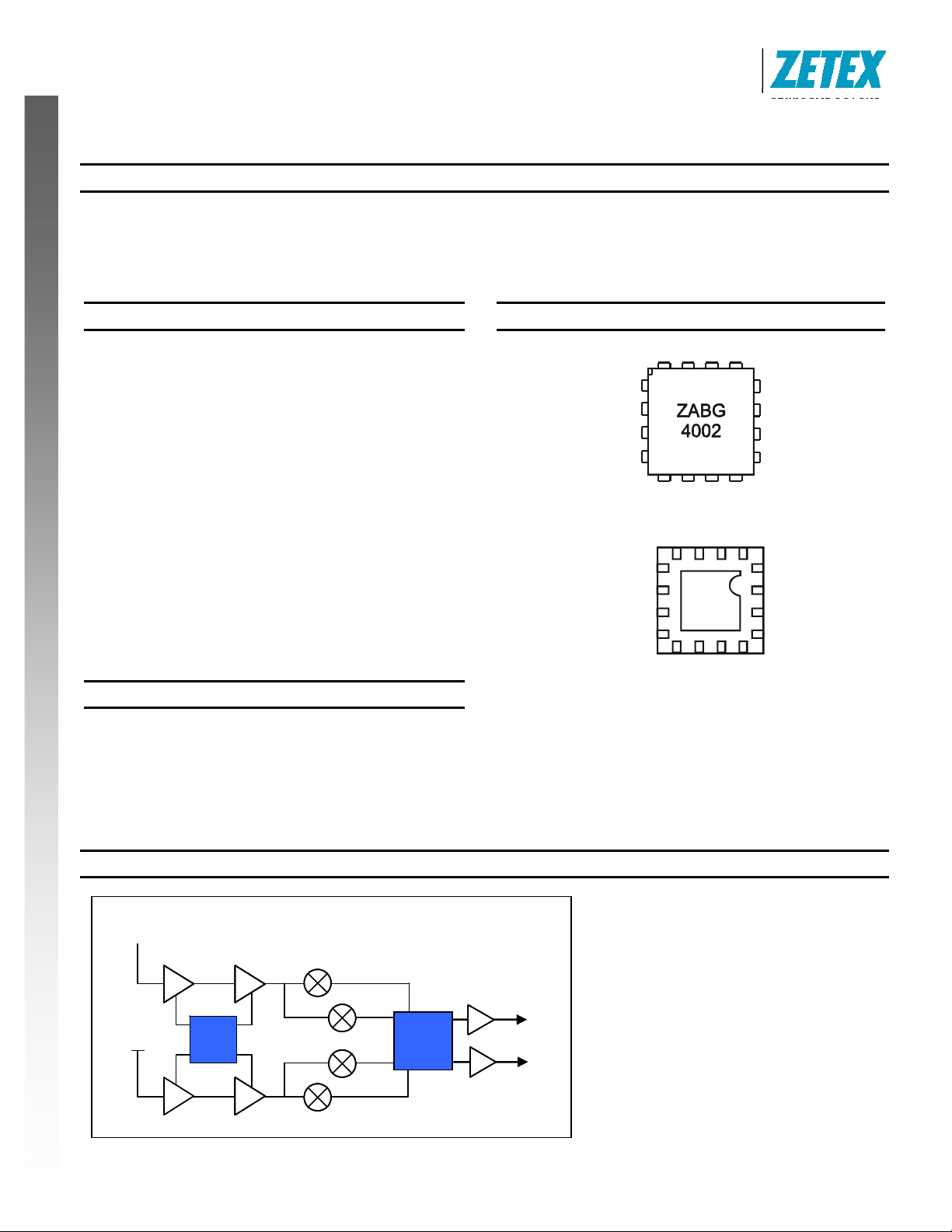
Pin Assignments
G2
V
CC
GND
G1
D1
V
CC
C
NB1
SUB
NB2
C
C
Top View
C
SUB
Bottom View
D3
R
G3D2
D4
G4
R
CAL1
CAL2
Single Universal LNB System Diagram
Gain stages
Gain stages
GaAs FET’s
GaAs FET’s
Vertical
Vertical
ZABG
ZABG
ZABG
ZABG
4002
4002
6002
6002
Horizontal
Horizontal
ZABG4002
Document number: DS32047 Rev. 2 - 2
Down
Down
Converter
Converter
IF Switc hing, gain
IF Switc hing, gain
and control
and control
ZXHF
ZXHF
ZXHF
ZXHF
5002
5002
5002
5002
www.diodes.com
1 of 7
February 2010
© Diodes Incorporated
Page 2
A
f
Device Description
The ZABG series of devices are designed to meet the bia s
requirements of GaAs and HEMT FETs commonly used i n
satellite receiver LNBs with a minimum of external
components whilst operating from a minimal voltage supp ly
and using minimal current.
The ZABG4002 provides four FET bias stages, arranged in
two pairs of two. Resistors connected to pins Rcal1 and
Rcal2 set the FET drain currents of each pair over the range
of 0 to 15mA, allowing input FETs to be biased for optimum
noise and amplifier FETs for optimum gain.
Drain voltages of all stages are set at 2.0V. The drain
supplies are current limited to approximately 5% above the
operating currents set by the Rcal resistors.
As an additional feature the Rcal pins can also be used as
logic inputs to disable pairs of FETs as part of a power
management scheme or simply an alternative to LNA
switching. Driven to a logic high (>3.0V), the inputs disable
NEW PRODUCT
their associated FET bias stages by switching gate feeds to -
2.5V and drain feeds open circuit.
Depletion mode FETs require a negative voltage bias supply
when operated in grounded source circuits. The ZABG4002
includes an integrated low noise switched capac itor DC-DC
converter generating a regulated output of -2.5V to allow
single supply operation.
Product Line o
Diodes Incorporated
ZABG4002
To facilitate the design of efficient low voltage 3.3V LNB
systems and to maintain compatibility with higher voltage
legacy designs, the ZABG4002 is capable of operating within
the supply of 3.0V to 8V.
These devices are unconditionally stable ov er the full working
temperature with the FETs in place, subject to the i nclusion of
the recommended gate and drain capacitors. These ensure
RF stability and minimal injected noise.
It is possible to use less than the devices full complement of
FET bias controls, unused drain and gate connections can be
left open circuit without affecting operation of the remaining
bias circuits.
To protect the external FETs the circuits have been designed
to ensure that, under any conditions including po wer up/down
transients, the gate drive from the bias circuits cannot exceed
-3V. Additionally each stage has its own individual current
limiter. Furthermore if the negative rail experiences a fault
condition, such as overload or short circuit, the drain supply to
the FETs will shut down avoiding excessive current flow.
To minimise PCB space ZABG4002 is packaged i n the 16 pin
3mm x 3mm QFN package.
Device operating temperature is -40°C to 85°C to suit a wide
range of environmental conditions.
ZABG4002
Document number: DS32047 Rev. 2 - 2
2 of 7
www.diodes.com
February 2010
© Diodes Incorporated
Page 3
A
f
)
)
)
)
)
)
)
)
)
Maximum Ratings
Parameter Rating Unit
Supply Voltage -0.6 to +10 V
Supply Current 80 mA
Power Dissipation 500 mW
Operating Temperature Range -40 to +85 °C
Storage Temperature Range -40 to +150 °C
Product Line o
Diodes Incorporated
ZABG4002
Electrical Characteristics (Measured at T
= 25°C, VCC = 3.3V (note 1), R
AMB
CAL
1 = R
2 = 39k (setting ID to 10mA) unless otherwise stated)
CAL
Parameter Conditions Symbol Min. Typ. Max. Unit
Operating Voltage Range
(note 1)
Supply Current
Substrate Voltage
Oscillator Frequency F
NEW PRODUCT
V
I
= ID2 = ID3 = ID4 = 0 ICC 1.2 4.0 mA
D1
ID1 = ID2 = ID3 = ID4 = 10mA I
I
= 0 V
CSUB
I
= -200uA V
CSUB
3.0 8.0 V
CC
42 44 mA
CC(L
CSUB
-2.55 -2.0 V
CSUB(L
150 240 600 kHz
OSC
-3.0 -2.65 -2.0 V
Gate Characteristics
Gate (G1 to G4)
Current Range IG -100 +500 uA
Voltage Low ID = 12mA, IG = -10uA V
Voltage High ID = 8mA, IG = 0 V
I
= 0, IG = -10uA,
Voltage Disabled
D
V
RCAL
= 3.0V
-3.0 -2.5 -2.0 V
G(L
0 0.7 1.0 V
G(H
V
-3.0 -2.5 -2.0 V
G(DIS)
Drain Characteristics
Drain (D1 to D4)
Current Range ID 0 15 mA
Current Operating Standard Application Circuit I
Current Disabled VD = 0, V
= 3.0V I
RCAL
Voltage Operating ID = 10mA V
delta ID vs VCC V
delta ID vs TOP T
delta VD vs VCC V
delta VD vs TOP T
R
(1 and 2)
CAL
= 3.3 to 8.0V dID/dVCC 1.2 %/V
CC
= -40°C to +85°C dID/dTOP 0.05 %/°C
OP
= 3.3 to 8.0V dVD/dVCC 0.05 %/V
CC
= -40°C to +85°C dVD/dTOP 50 ppm/°C
OP
Disable Threshold V
Input Current V
= 3.0V I
RCAL
8 10 12 mA
D(OP
10 uA
D(DIS
1.8 2.0 2.2 V
D(OP
RCAL(DIS
RCAL(DIS
1.8 2.7 3.0 V
1.7 10 uA
Output Noise
C
Drain Voltage
Gate Voltage
Notes: 1. The two Vcc pins are internally connected, only one of the pins needs to be powered for the device to function. See applications section for further
information.
2. ESD sensitive, handling precautions are recommended.
3. The negative bias voltages are generated on-chip using an internal oscillator. Two external capacitors, C
purpose.
4. The package (QFN1633) exposed pad must either be connected to Csub or le ft open circuit.
5. The characteristics are measured using two external reference resistors R
sets the drain current of FETs 1 and 3, resistor R
6. Noise voltage measurements are made with FETs and gate and drain capacitors of value 10nF in place. Noise voltages are not measured in production.
GATE-GND
C
DRAIN-GND
C
GATE-GND
C
DRAIN-GND
ZABG4002
Document number: DS32047 Rev. 2 - 2
= 10nF,
= 10nF
= 10nF,
= 10nF
CAL2
V
V
and R
sets the drain currents of FETs 2 and 4.
www.diodes.com
CAL1
3 of 7
0.02 Vpk-pk
D(NOISE)
0.005 Vpk-pk
G(NOISE)
of value 39k, wired from pins R
CAL2
and C
NB
of value 47nF are required for this
SUB
to ground. Resistor R
CAL1/2
February 2010
© Diodes Incorporated
CAL1
Page 4

A
Product Line o
f
Diodes Incorporated
ZABG4002
Typical Characteristics (Measured at T
ZA BG4002 Drain Current vs R
15
10
Drain Current (mA)
5
0
10 100 1000
R
NEW PRODUCT
ZABG4002 Drain Drain Current vs Temperature
20
18
16
14
12
10
8
Drain Current (mA)
6
4
2
0
-40-200 20406080
ZA B G 4002 Subs trate Volt a ge vs Substrate Current
Temperature (°C)
= 25°C, VCC = 3.3V, R
AMB
CAL
(k)
CAL
CAL
1 = R
2 = 39k (setting ID to 10mA) unless otherwise stated)
CAL
ZA BG 4002 Drain Voltage vs Drain Current
2.2
2.1
2
Drain Voltage (V)
1.9
1.8
0 5 10 15
Drain Current ( m A )
ZABG4002 Drain Voltage vs Temperature
2.3
2.2
2.1
2
Drain Voltage (V)
1.9
1.8
1.7
-40 -20 0 20 40 60 80
Temperat ur e (°C)
-2
-2.2
-2.4
-2.6
Substrate Voltage (V)
-2.8
-3
0 50 100 150 200 250
Substrate Cur r ent ( uA )
ZABG4002
Document number: DS32047 Rev. 2 - 2
4 of 7
www.diodes.com
February 2010
© Diodes Incorporated
Page 5

A
f
Applications Circuit
NEW PRODUCT
JF1
* Str ipline Elemen t s
L*
C* C1
L*
C*
10nF
C2
10nF
G2
Vcc
Gnd
CNB
47nF
G1D3Vcc
ZABG4002
Cnb1
CSUB
47nF
Product Line o
Diodes Incorporated
D1
G3D2
D4
G4
Rcal1
Cnb2
Csub
Rcal2
RCAL2
39k
RCAL1
39k
ZABG4002
Vcc
Applications Information
Above is a partial applications circuit for the ZABG4002 showing all exter nal components needed for biasin g one of the four FET
stages available. Each bias stage is provided with a gate and drain pin. The drain pin provides a regulated 2.0V supply that
includes a drain current monitor. The drain current taken by the external FET is compare d with a user selected level, gener ating a
signal that adjusts the gate voltage of the FET to obtain the required drain current. If for an y reason, an attempt is made to draw
more than the user set drain current from the drain pin, the drain voltage will be reduced to ensure e xcess current is not taken.
The gate pin drivers are also current limited.
The bias stages are split up into two pairs, with the drain current of each pa ir set by an external R
currents of stages 1 and 3, whilst R
2 sets the drain currents of stages 2 and 4. This all o ws the optimisation of drai n currents for
CAL
resistor. R
CAL
differing tasks such as input stages where noise can be critical and later amplifi er stages where gain may be more important. A
graph showing the relationship between the value of R
datasheet. The R
pins can also be used as logic inputs. If set to a logic high state (>3.0V), the associated FET bias stages are
CAL
and ID is provided in the Typical Characteristics section of this
CAL
disabled, driving gate pins to -2.5V and switching drain pins open-circuit. This feature can be used as part of a power
management system that turns off any unwanted stages in a multi input receiver.
The ZABG4002 includes a switched capacitor DC-DC co nverter that is used to generate the negative supply required to bias
depletion mode FETs used in common source circuit configuration as shown above. This converter us es two external capacitors,
C
the charge transfer capacitor and C
NB
the output reservoir capacitor. The circuit provides a regulated -2.5V supply both for
SUB
gate driver use and for external use if required (for extra discrete bias stages, mi xer bias, local oscillator bias etc.). The -2.5V
supply is available from the C
SUB
pin.
If any bias stages are not required, their gate and drain pins may be le ft open circuit. If all bias stages associated with an R
resistor are not required, then this resistor may be omitted.
To ease PCB layout, the pinout for the ZABG4002 includes two Vcc pins. T hese pins are internally connected so o nly one of the
pins needs to be powered for the device to f unction. It is probable that the e xtra pin will help avoid the need for trace cross-over
components or ground plane disruption from reverse side PCB links. Note that the e xposed pad of t he package must be either left
floating or connected to Csub.
1 sets the drain
CAL
CAL
ZABG4002
Document number: DS32047 Rev. 2 - 2
5 of 7
www.diodes.com
February 2010
© Diodes Incorporated
Page 6

A
f
Package Outline Dimensions
Note: Controlling dimensions are in millimetres. Approximate dimensions are provided in inches.
The package appearance may vary as shown, for further details please contact your local Diodes sales office.
NEW PRODUCT
D
Pin #1 ID
e
b
E
E2
Z
A1
A3
A
L
D2
Product Line o
Diodes Incorporated
ZABG4002
QFN16 3x3
Dim Min Max
A 0.55 0.65
A1 0.00 0.05
A3 0.15 Typ
b 0.18 0.28
D 2.95 3.05
D2 1.40 1.60
e 0.50 BSC
E 2.95 3.05
E2 1.40 1.60
L 0.35 0.45
Z 0.625 Typ
All Dimensions in mm
Ordering Information (Note x)
Device Package
Reel Size
(inches)
ZABG4002JA16TC QFN1633 13 8 3000
Tape Width
(mm)
Quantity
(per reel)
Marking Information
ZABG
4002
YYWW
ZABG4002
Document number: DS32047 Rev. 2 - 2
6 of 7
www.diodes.com
Pin 1
Part Name
Date Code
Year/Week
February 2010
© Diodes Incorporated
Page 7

A
Product Line o
f
Diodes Incorporated
ZABG4002
DIODES INCORPORATED MAKES NO WARRANTY OF ANY KIND, EXPRESS OR IMPLIED, WITH REGARDS TO THIS DOCUMENT,
INCLUDING, BUT NOT LIMITED TO, THE IMPLIED WARRANTIES OF MERCHANTABILITY AND FITNESS FOR A PARTICULAR PURPOSE
(AND THEIR EQUIVALENTS UNDER THE LAWS OF ANY JURISDICTION).
Diodes Incorporated and its subsidiaries reserve the right to make modifications, enhancements, improvements, corrections or other changes
without further notice to this document and any product described herein. Diodes Incorporated does not assume any liability arising out of the
application or use of this document or any product described herein; neither does Diodes Incorporated convey any license under its patent or
trademark rights, nor the rights of others. Any Customer or user of this document or products described herein in such applications shall assume
all risks of such use and will agree to hold Diodes Incorporated and all the companies whose products are represented on Diodes Incorporated
website, harmless against all damages.
Diodes Incorporated does not warrant or accept any liability whatsoever in respect of any products purchased through unauthorized sales channel.
Should Customers purchase or use Diodes Incorporated products for any unintended or unauthorize d application, Customers shall indemnify and
hold Diodes Incorporated and its representatives harmless against all claims, damages, expenses, and attorney fees arising out of, directly or
indirectly, any claim of personal injury or death associated with such unintended or unauthorized application.
Products described herein may be covered by one or more United States, international or foreign patents pending. Product names and markings
noted herein may also be covered by one or more United States, international or foreign trademarks.
NEW PRODUCT
Diodes Incorporated products are specifically not authorized for use as critical components in life support devices or systems without the express
written approval of the Chief Executive Officer of Diodes Incorporated. As used herein:
A. Life support devices or systems are devices or systems which:
1. are intended to implant into the body, or
labeling can be reasonably expected to result in significant injury to the user.
B. A critical component is any component in a life support device or system whose failure to perform can be reasonably expected to cause the
failure of the life support device or to affect its safety or effectiveness.
Customers represent that they have all necessary expertise in the safety and regulatory ramifications of their life support devices or systems, and
acknowledge and agree that they are solely responsible for all legal, regulatory and safety-related requirements concerning their products and any
use of Diodes Incorporated products in such safety-critical, life support devices or systems, notwithstanding any devices- or systems-related
information or support that may be provided by Diodes Incorporated. Further, Customers must fully indemnify Diodes Incorporated and its
representatives against any damages arising out of the use of Diodes Incorporated products in such safety-critical, life support devices or systems.
Copyright © 2010, Diodes Incorporated
www.diodes.com
2. support or sustain life and whose failure to perform when properly used in accordance with instructions for use provided in the
IMPORTANT NOTICE
LIFE SUPPORT
ZABG4002
Document number: DS32047 Rev. 2 - 2
7 of 7
www.diodes.com
February 2010
© Diodes Incorporated
 Loading...