

Page 1
Features
Small, Surface Mount Package
Ideally suited for Automated Assembly Processes
Very Sharp Breakdown Characteristics
Very Tight Tolerance on Zener Breakdown Voltage
Totally Lead-Free & Fully RoHS Compliant (Notes 1 & 2)
Halogen and Antimony Free. “Green” Device (Note 3)
UDZ3V6B-UDZ15B
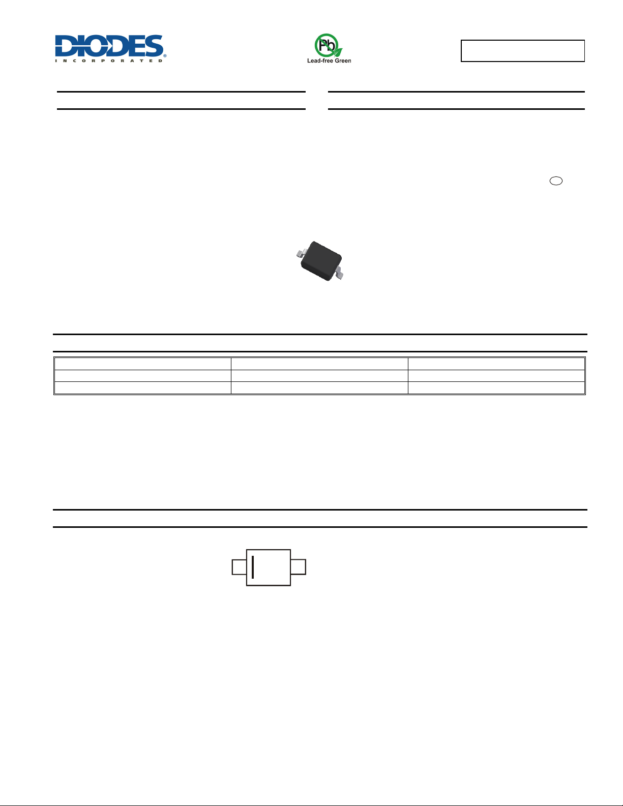
SURFACE MOUNT PRECISION ZENER DIODE
Mechanical Data
Case: SOD323
Case Material: UL Flammability Classification Rating 94V-0
Moisture Sensitivity: Level 1 per J-STD-020D
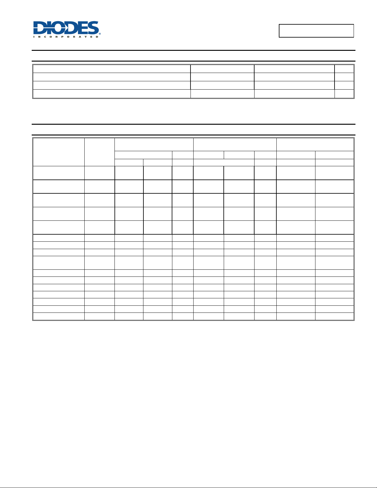
Terminal Connections: Cathode Band
Terminals: Finish - Matte Tin annealed over Alloy 42
leadframe. Solderable per MIL-STD-202, Method 208
Weight: 0.004 grams (approximate)
Top View
e3
Ordering Information (Note 4)
Device
(Type Number)-7*
(Type Number)-13* (Note 5)
* For (Type Number), please see the Electrical Characteristics Table. Example: 6.2V Zener = UDZ6V2B-7.
Notes: 1. No purposely added lead. Fully EU Directive 2002/95/EC (RoHS) & 2011/65/EU (RoHS 2) compliant.
2. See http://www.diodes.com/quality/lead_free.html for more information about Diodes Incorporated’s definitions of Halogen- and Antimony-free, "Green"
and Lead-free.
3. Halogen- and Antimony-free "Green” products are defined as those which contain <900ppm bromine, <900ppm chlorine (<1500ppm total Br + Cl) and
<1000ppm antimony compounds.
4. For packaging details, go to our website at http://www.diodes.com/products/packages.html
5. Devices are readily available on 13” reels for select voltages only. For other voltages, devices can be made available on 13” reels upon request. Please
Contact your Diodes Inc. sales representative for additional details.
Packaging Shipping
SOD323 3000/Tape & Reel
SOD323 10000/Tape & Reel
Marking Information
UDZ3V6B-UDZ15B
Document number: DS30290 Rev. 15 - 2
XX
xx = Product Type Marking Code
(See Electrical Characteristics Table)
1 of 5
www.diodes.com
December 2013
© Diodes Incorporated
Page 2
UDZ3V6B-UDZ15B
Thermal Characteristics
Characteristic Symbol Value Unit
Power Dissipation (Note 6)
Thermal Resistance Junction to Ambient Air (Note 6)
Operating and Storage Temperature Range
PD
R
T
J, TSTG
JA
200 mW
625
-65 to +150
C/W
C
Electrical Characteristics (@T
Type
Number
Marking
Code
= +25°C, unless otherwise specified.)
A
Zener Voltage Range
Maximum Zener Impedance
(Note 7)
V
IZT Z
ZT @ IZT
ZT @ IZT
(Note 8)
ZZK @ IZK IZK IR V
(Note 7)
R
Maximum Reverse Current
Min (V) Max (V) mA Ω mA uA V
UDZ3V6B
(Note 9)
UDZ3V9B
(Note 9)
UDZ4V3B
(Note 9)
UDZ4V7B
(Note 9)
UDZ5V1B
(Note 9)
B7 3.600 3.845 5 100 1000 1.0 10 1.0
B8 3.890 4.160 5 100 1000 1.0 5 1.0
B9 4.170 4.430 5 100 1000 1.0 5 1.0
BA 4.550 4.750 5 100 800 0.5 2 1.0
BB 4.980 5.200 5 80 500 0.5 2 1.5
UDZ5V6B BC 5.490 5.730 5 60 200 0.5 1 2.5
UDZ6V2B BD 6.060 6.330 5 60 100 0.5 1 3.0
UDZ6V8B BE 6.650 6.930 5 40 60 0.5 0.5 3.5
UDZ7V5B
(Note 9)
BF 7.280 7.600 5 30 60 0.5 0.5 4.0
UDZ8V2B BG 8.020 8.360 5 30 60 0.5 0.5 5.0
UDZ9V1B BH 8.850 9.230 5 30 60 0.5 0.5 6.0
UDZ10B BI 9.770 10.210 5 30 60 0.5 0.1 7.0
UDZ11B BJ 10.760 11.220 5 30 60 0.5 0.1 8.0
UDZ12B BK 11.740 12.240 5 30 80 0.5 0.1 9.0
UDZ13B BL 12.910 13.490 5 37 80 0.5 0.1 10.0
UDZ15B BM 14.340 14.980 5 42 80 0.5 0.1 11.0
Notes: 6. Part mounted on FR-4 PC board with recommended pad layout, which can be found on our website at http://www.diodes.com/datasheets/ap02001.pdf.
7. Short duration pulse test used to minimize self-heating effect.
8. The Zener impedances (Z
9. AEC-Q101 qualified
UDZ3V6B-UDZ15B
Document number: DS30290 Rev. 15 - 2
, ZZK) are measured by superimposing a minute alternating current on the regulated current (IZ).
ZT
2 of 5
www.diodes.com
December 2013
© Diodes Incorporated
Page 3

P
P
OWER
P
TIO
N
TANT
O
US FOR
R
CUR
RENT
R CUR
RENT
R CUR
RENT
N
R C
URR
N
T
250
R = 625°C/W
JA
200
Note 6
1,000
(mA)
100
UDZ3V6B-UDZ15B
(mW)
A
150
D
10
WA
DISSI
100
,
D
50
100m
10m
0
0
40 80 160
T , AMBIENT TEMPERATURE (°C)
A
Fig. 1 Power Derating Curve
120
200
1.0
ANE
0.1
0.01
F
I , INS
0
V , INSTANTANEOUS FORWARD VOLTAGE (V)
F
0.2
0.4
0.6 0.8
Fig. 2 Typical Forward Charact eristics
100m
10m
1.0
1.2
(A)
1m
Z
I, ZENE
100n
V , ZENER VOLTAGE (V)
Z
5.0 7.0 9.02.0 3.01.00.0
4.0 6.0 8.0 10.0
Fig. 3 Typical Zener Breakdown Characteristics,
UDZ3V6B - UDZ8V2B
100
10
(mA)
(A)
1m
Z
I, ZENE
100n
8.0 10.0 12.0 14.0
9.0 11.0 13.0
V , ZENER VOLTAGE (V)
Z
Fig. 4 Typical Zener Breakdown Characteristics,
UDZ10B - UDZ13B
30
25
20
T = 25°C
A
E
15
E
10
0V Bias
1V Bias
Z
I, ZE
0.1
10
12
14
V , ZENER VOLTAGE (V)
Z
16
18
20
Fig. 5 Typical Zener Breakdown Characteristics, UDZ15B
UDZ3V6B-UDZ15B
Document number: DS30290 Rev. 15 - 2
3 of 5
www.diodes.com
T
C , TOTAL CAPACITANCE (pF)
5
2V Bias
0
46810121416
V , NOMINAL ZENER VOLTAGE (V)
Z
Fig. 6 Typical Total Capacitance
vs. Nominal Zener Voltage
December 2013
© Diodes Incorporated
Page 4

T
C
TEMPER
T
U
R
C
O
F
F
C
T
T
C
TEMP
R
T
U
RE C
OEF
F
C
T
0.12
0.10
IEN
0.08
I
0.06
E
0.04
E
0.02
A
0
-0.02
Z
OF ZENER VOLTAGE (%/°C)
-0.04
of V ,
-0.06
-0.08
0610
Fig. 7 Typical Temperature Coefficient of
Zener Voltage vs. Zener Voltage, UDZ6V2B-UDZ10B
42
V , ZENER VOLTAGE (V)
Z
8
0.12
0.10
IEN
0.08
I
0.06
0.04
0.02
A
E
-0.02
Z
OF ZENER VOLTAGE (%/°C)
-0.04
of V ,
-0.06
-0.08
Package Outline Dimensions
Please see AP02002 at http://www.diodes.com/datasheets/ap02002.pdf for latest version.
C
H
B
M
A
K
L
J
UDZ3V6B-UDZ15B
0
10
Zener Voltage vs. Zener Voltage, UDZ10B-UDZ15B
12
Fig. 8 Typical Temperature Coefficient of
All Dimensions in mm
14
V , ZENER VOLTAGE (V)
Z
SOD323
Dim Min Max
A 0.25 0.35
B 1.20 1.40
C 2.30 2.70
H 1.60 1.80
J 0.00 0.10
K 1.0 1.1
L 0.20 0.40
M 0.10 0.15
0° 8°
16 20
18
Suggested Pad Layout
Please see AP02001 at http://www.diodes.com/datasheets/ap02001.pdf for the latest version.
UDZ3V6B-UDZ15B
Document number: DS30290 Rev. 15 - 2
Y
X1
X
G
4 of 5
www.diodes.com
Dimensions Value (in mm)
G 1.520
X 0.590
X1 2.700
Y 0.450
December 2013
© Diodes Incorporated
Page 5

IMPORTANT NOTICE
DIODES INCORPORATED MAKES NO WARRANTY OF ANY KIND, EXPRESS OR IMPLIED, WITH REGARDS TO THIS DOCUMENT,
INCLUDING, BUT NOT LIMITED TO, THE IMPLIED WARRANTIES OF MERCHANTABILITY AND FITNESS FOR A PARTICULAR PURPOSE
(AND THEIR EQUIVALENTS UNDER THE LAWS OF ANY JURISDICTION).
Diodes Incorporated and its subsidiaries reserve the right to make modifications, enhancements, improvements, corrections or other changes
without further notice to this document and any product described herein. Diodes Incorporated does not assume any liability arising out of the
application or use of this document or any product described herein; neither does Diodes Incorporated convey any license under its patent or
trademark rights, nor the rights of others. Any Customer or user of this document or products described herein in such applications shall assume
all risks of such use and will agree to hold Diodes Incorporated and all the companies whose products are represented on Diodes Incorporated
website, harmless against all damages.
Diodes Incorporated does not warrant or accept any liability whatsoever in respect of any products purchased through unauthorized sales channel.
Should Customers purchase or use Diodes Incorporated products for any unintended or unauthorized application, Customers shall indemnify and
hold Diodes Incorporated and its representatives harmless against all claims, damages, expenses, and attorney fees arising out of, directly or
indirectly, any claim of personal injury or death associated with such unintended or unauthorized application.
Products described herein may be covered by one or more United States, international or foreign patents pending. Product names and markings
noted herein may also be covered by one or more United States, international or foreign trademarks.
This document is written in English but may be translated into multiple languages for reference. Only the English version of this document is the
final and determinative format released by Diodes Incorporated.
LIFE SUPPORT
Diodes Incorporated products are specifically not authorized for use as critical components in life support devices or systems without the express
written approval of the Chief Executive Officer of Diodes Incorporated. As used herein:
A. Life support devices or systems are devices or systems which:
1. are intended to implant into the body, or
2. support or sustain life and whose failure to perform when properly used in accordance with instructions for use provided in the
labeling can be reasonably expected to result in significant injury to the user.
B. A critical component is any component in a life support device or system whose failure to perform can be reasonably expected to cause the
failure of the life support device or to affect its safety or effectiveness.
Customers represent that they have all necessary expertise in the safety and regulatory ramifications of their life support devices or systems, and
acknowledge and agree that they are solely responsible for all legal, regulatory and safety-related requirements concerning their products and any
use of Diodes Incorporated products in such safety-critical, life support devices or systems, notwithstanding any devices- or systems-related
information or support that may be provided by Diodes Incorporated. Further, Customers must fully indemnify Diodes Incorporated and its
representatives against any damages arising out of the use of Diodes Incorporated products in such safety-critical, life support devices or systems.
Copyright © 2013, Diodes Incorporated
www.diodes.com
UDZ3V6B-UDZ15B
UDZ3V6B-UDZ15B
Document number: DS30290 Rev. 15 - 2
5 of 5
www.diodes.com
December 2013
© Diodes Incorporated
 Loading...