Page 1

f
‡
‡
‡
Description
The TLV431 is a three terminal adjustable shunt regulator offering
excellent temperature stability and output current handling capability
up to 20mA. The output voltage may be set to any chosen voltage
between 1.24 and 18 volts by selection of two external divider
resistors.
The TLV431 can be used as a replacement for zener diodes in many
applications requiring an improvement in zener performance.
The TLV431 is available in 3 grades with initial tolerances of 1%,
0.5%, and 0.2% for the A, B and T grades respectively.
Features
• Low Voltage Operation V
• Temperature range -40 to +125°C
• Reference Voltage Tolerance at +25°C
0.2% TLV431T
0.5% TLV431B
1% TLV431A
• Typical temperature drift
4 mV (0°C to +70°C)
6 mV (-40°C to +85°C)
11mV (-40°C to +125°C)
• 80µA Minimum cathode current
• 0.25Ω Typical Output Impedance
• Adjustable Output Voltage V
• Lead-Free Finish; RoHS Compliant (Notes 1 & 2)
• Halogen and Antimony Free. “Green” Device (Note 3)
• Qualified to AEC-Q100
= 1.24V
REF
REF
to 18V
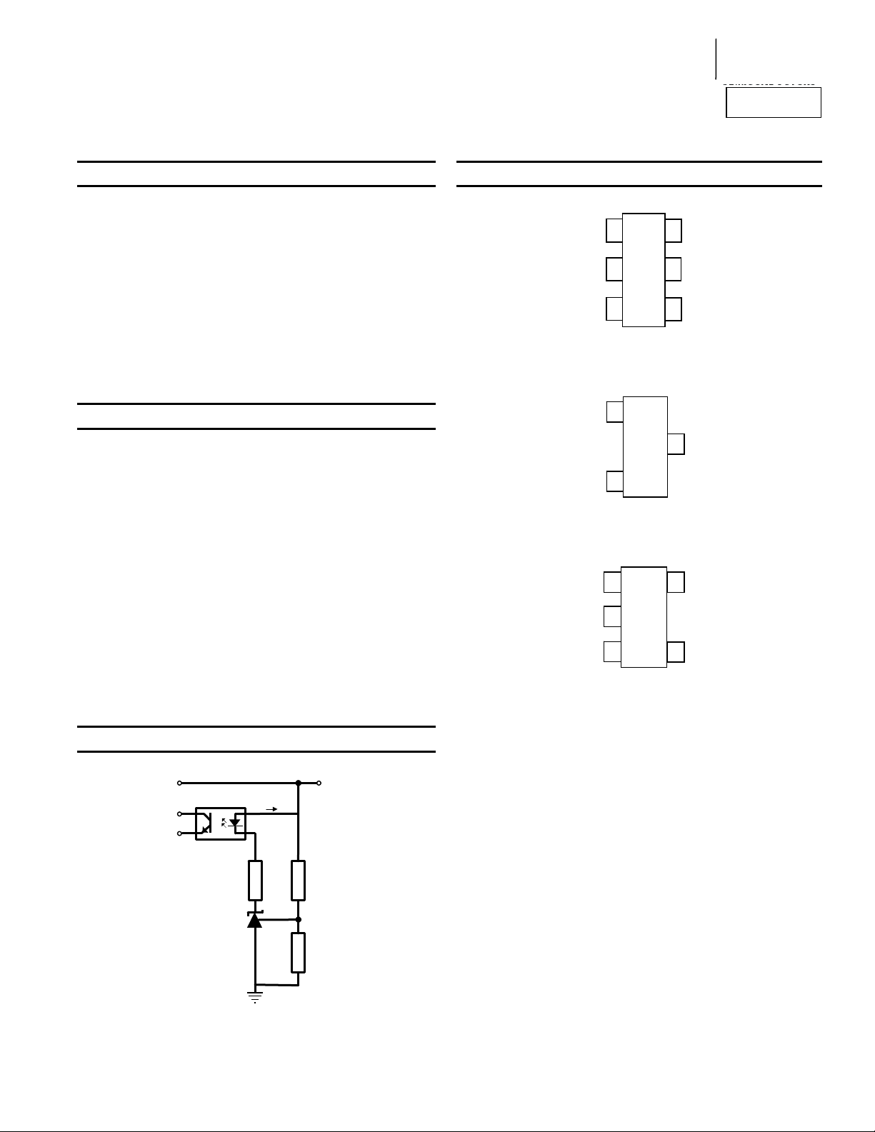
Typical Application Circuit
Secondary side
regulated supply
Primary side
controller
Optocoupler
I
F
3.3 V
1.24V COST EFFECTIVE SHUNT REGULATOR
Pin Assignments
CATHODE 1
CATHODE
CATHODE
‡ Pin should be left floating or connect to anode
A Product Line o
Diodes Incorporated
TLV431_H6 (SC70-6 [SOT363])
2
N/C
REF
TLV431_F (SOT23)
REF 1
3
(Top View)
6 ANODE
5 NC
4 NC
3 ANODE
2
(Top View)
3
(Top View)
5 ANODE
4 REF
TLV431_E5 (SOT25)
N/C 1
2
N/C
TLV431
R3
TLV431
GND
Notes: 1. EU Directive 2002/95/EC (RoHS) & 2011/65/EU (RoHS 2) compliant. All applicable RoHS exemptions applied.
2. See http://www.diodes.com for more information about Diodes Incorporated’s definitions of Halogen- and Antimony-free, "Green" and Lead-free.
3. Halogen- and Antimony-free "Green” products are defined as those which contain <900ppm bromine, <900ppm chlorine (<1500ppm total Br + Cl) and
<1000ppm antimony compounds.
R1
R2
TLV431
Document number: DS32088 Rev. 6 - 2
1 of 14
www.diodes.com
October 2012
© Diodes Incorporated
Page 2

f
A Product Line o
Diodes Incorporated
TLV431
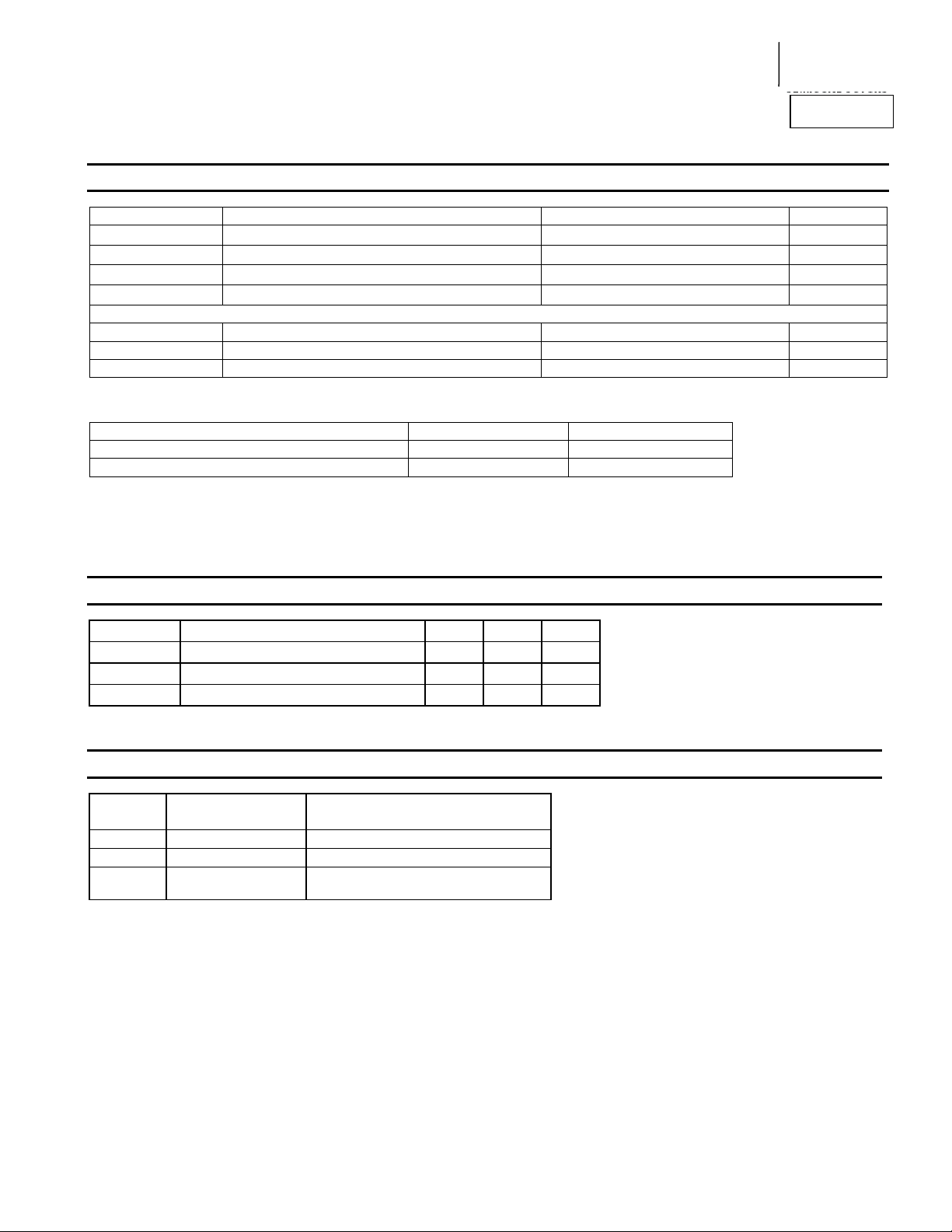
Absolute Maximum Ratings (@T
Symbol Parameter Rating Unit
VKA
IKA
I
REF
VIN
ESD Susceptibility
HBM Human Body Model 4 kV
MM Machine Model 400 V
CDM Charged Device Model 1 kV
(Semiconductor devices are ESD sensitive and may be damaged by exposure to ESD events. Suitable ESD precautions should be taken when handling and
transporting these devices.)
Operating Junction Temperature -40 to +150 °C
Storage Temperature -65 to +150 °C
Operation above the absolute maximum rating may cause device failure.
Operation at the absolute maximum ratings, for extended periods, may reduce device reliability.
Unless otherwise stated voltages specified are relative to the ANODE pin.
These are stress ratings only. Operation outside the absolute maximum ratings may cause device failure.
Cathode Voltage 20 V
Continuous Cathode Current -20 to +20 mA
Reference Input Current Range -0.05 to +3 mA
Input Supply Voltage (Relative to Ground) -0.03 to +18 V
Parameter Rating Unit
Recommended Operating Conditions (@T
Symbol Parameter Min Max Units
VKA
IKA
TA
Cathode Voltage
Cathode Current 0.1 15 mA
Operating Ambient Temperature Range
= +25°C, unless otherwise specified.)
A
= +25°C, unless otherwise specified.)
A
V
REF
-40 +125 °C
18 V
Package Thermal Data
P
Package
SOT23 380°C/W 330mW
SOT25 250°C/W 500mW
SC70-6
(SOT363)
θ
JA
380°C/W 330mW
T
= +25°C, TJ = +150°C
A
TLV431
Document number: DS32088 Rev. 6 - 2
DIS
2 of 14
www.diodes.com
October 2012
© Diodes Incorporated
Page 3

f
A Product Line o
Diodes Incorporated
TLV431
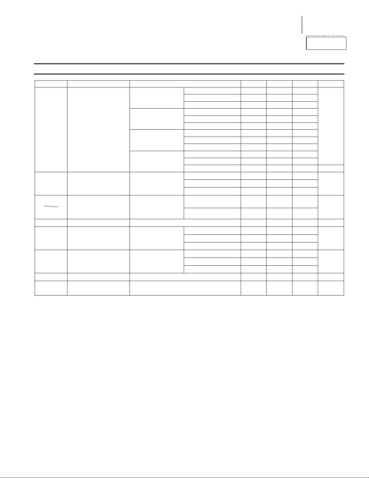
Electrical Characteristics (@T
Symbol Parameter Conditions Min Typ Max Units
Reference Voltage
Deviation of reference
voltage over full
temperature range
Ratio of change in
reference voltage to the
change in cathode
voltage
Reference Input Current
deviation over full
I
REF
temperature range
Minimum cathode
current for regulation
Off state current
Dynamic output
impedance
V
REF
V
REF(dev)
ΔV
ΔV
I
REF
I
REF(dev)
I
KMIN
I
K(OFF)
ZKA
REF
KA
= +25°C, unless otherwise specified.)
A
= V
REF
REF
REF
REF
REF
,
,
,
,
V
KA
= +25°C
T
A
VKA = V
= 0 to +70°C
T
A
VKA = V
= -40 to +85°C
T
A
VKA = V
= -40 to +125°C
T
A
VKA = V
TLV431A 1.228 1.24 1.252
TLV431B 1.234 1.24 1.246
TLV431T 1.2375 1.24 1.2425
TLV431A 1.221 1.259
TLV431B 1.227 1.253
TLV431T 1.230 1.250
TLV431A 1.215 1.265
TLV431B 1.224 1.259
TLV431T 1.228 1.252
TLV431A 1.209 1.271
TLV431B 1.221 1.265
TLV431T 1.224 1.255
= 0 to +70°C
T
A
TA = -40 to +85°C
TA = -40 to +125°C
6V -1.5 -2.7
V
KA
for V
REF
to
18V -1.5 -2.7
R1 = 10kΩ, R2 = OC
= 0 to +70°C
T
= 10kΩ,
R
1
R
= OC
2
VKA = V
REF
A
TA = -40 to +85°C
TA = -40 to +125°C
= 0 to +70°C
T
A
TA = -40 to +85°C
TA = -40 to +125°C
= 18V, V
V
KA
V
= V
KA
REF,
= 0.1 to 15mA
I
K
= 0V
REF
f = <1kHz
V
4 12
6 20
mV
11 31
mV/V
0.15 0.5 µA
0.05 0.3
0.1 0.4
µA
0.15 0.5
55 80
55 80
µA
55 100
0.001 0.1 µA
0.25 0.4 Ω
TLV431
Document number: DS32088 Rev. 6 - 2
3 of 14
www.diodes.com
October 2012
© Diodes Incorporated
Page 4

f
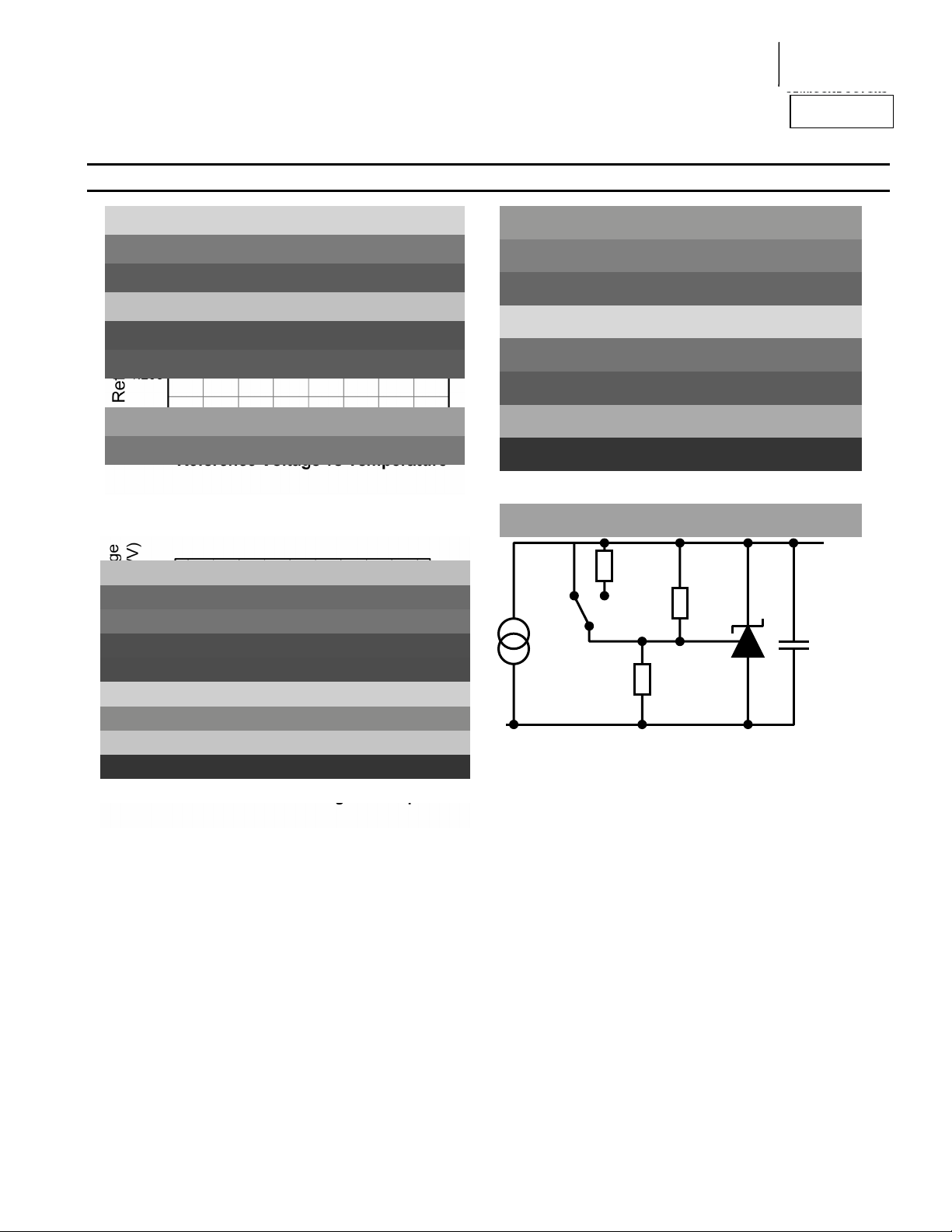
Typical Characteristics
A Product Line o
Diodes Incorporated
TLV431
56kΩ
75kΩ
I
K
O/P
S1
10mA
100nF
10kΩ
Test Circuit for V
TLV431
Document number: DS32088 Rev. 6 - 2
4 of 14
www.diodes.com
Measurement
REF
October 2012
© Diodes Incorporated
Page 5

f
Typical Characteristics (cont.)
A Product Line o
Diodes Incorporated
TLV431
TLV431
Document number: DS32088 Rev. 6 - 2
5 of 14
www.diodes.com
October 2012
© Diodes Incorporated
Page 6

f
Typical Characteristics (cont.)
A Product Line o
Diodes Incorporated
TLV431
3V
1kΩ
470µF
750Ω
O/P
Test Circuit for Input Noise Voltage
6.8kΩ
I
K
10µF
O/P
180Ω
5V
4.3kΩ
Test Circuit for Phase Shift and Gain
100µF
100Ω
100Ω
50Ω
O/P
Test Circuit for Reference Impedance
TLV431
Document number: DS32088 Rev. 6 - 2
www.diodes.com
6 of 14
© Diodes Incorporated
October 2012
Page 7

f
Typical Characteristics (cont.)
Pulse
Generator
A Product Line o
Diodes Incorporated
TLV431
O/P
Test Circuit for Pulse Response
TLV431
Document number: DS32088 Rev. 6 - 2
7 of 14
www.diodes.com
October 2012
© Diodes Incorporated
Page 8

f
A Product Line o
Diodes Incorporated
TLV431
Application Notes
In a conventional shunt regulator application (Figure 1), an external series resistor (R3) is connected between the supply voltage, VIN, and the
TLV431.
R
determines the current that flows through the load (IL) and the TLV431 (IK). The TLV431 will adjust how much current it sinks or “shunts” to
3
maintain a voltage equal to V
at least the minimum acceptable I
value. When the supply voltage is at its maximum and I
TLV431 is less than 15mA.
R
is determined by the supply voltage, (VIN), the load and operating current, (IL and IK), and the TLV431’s reverse breakdown voltage, VKA.
3
across its feedback pin. Since load current and supply voltage may vary, R3 should be small enough to supply
REF
to the TLV431 even when the supply voltage is at its minimum and the load current is at its maximum
KMIN
is at its minimum, R3 should be large enough so that the current flowing through the
L
VV
−
KAIN
R
=
3
and V
where
REFKA
= V
KA
II
+
KL
1VV
OUT
⎞
R
1
⎟
+×=
⎟
R
2
⎠
⎛
⎜
⎜
⎝
The values of R1 and R2 should be large enough so that the current flowing through them is much smaller than the current through R3 yet not
too large that the voltage drop across them caused I
The most frequent application of the TLV431 is in isolated low output voltage power supplies where the regulated output is galvanically isolated
from the controller. As shown in Figure 2 the TLV431 drives current, I
which is connected to the controller on the primary side of the power supply.
This completes the feedback path through the isolation barrier and ensures that a stable isolated supply is maintained.
Assuming a forward drop of 1.4V across the opto-coupler diode allows output voltages as low as 2.7V to be regulated.
Figure 1
affects the reference accuracy.
REF
, through the opto-coupler’s LED which in turn drives the isolated transistor
F
Regulated SupplyRegulated Supply
Optocoupler
To controller
To controller
TLV431
I
F
1R
⎛
⎜
REFOUT
R3
R1
R2
OUT
I
−
7.2V
(min)F
⎝
≥>
3R
⎞
+=
1VV
⎟
2R
⎠
−
(max)OUT
7.2V
mA15
GND
Figure 2. Using the TLV431 as the Regulating Element in an Isolated PSU
TLV431
Document number: DS32088 Rev. 6 - 2
8 of 14
www.diodes.com
October 2012
© Diodes Incorporated
Page 9

f
A Product Line o
Diodes Incorporated
TLV431
Application Notes (cont.)
Printed Circuit Board Layout Considerations
The TLV431 in the SOT25 package has the die attached to pin 2, which results in an electrical contact between pin 2 and pin 5. Therefore, pin 2
of the SOT25 package must be left floating or connected to pin 5.
TLV431 in the SC70-6 (SOT363) package has the die attached to pin 2 and 5, which results in an electrical contact between pins 2, 5 and pin 6.
Therefore, pins 2 and 5 must be left floating or connected to pin 6.
Other Applications of the TLV431
Vin
R3
TLV431
I
B
0.1µF
R4
ZXTP2039F
C1
Q1
I
SH
Vout
1R
⎛
⎜
R1
V
REF
⎛
R2
⎜
⎜
h
⎝
REFOUT
⎝
VV
−
3R
=
+
V
BE
4R =
I
B
⎞
I
SH
⎟
B
⎟
(min)FE
⎠
⎞
+=
1VV
⎟
2R
⎠
OUTIN
II
BSH
mA15I
≤<
GND
It may at times be required to shunt-regulate more current than the 15mA that the TLV431 is capable of.
Figure 3 shows how this can be done using transistor Q1 to amplify the TLV431’s current. Care needs to be taken that the power dissipation
and/or SOA requirements of the transistor is not exceeded.
A very effective and simple series regulator can be implemented as shown in Figure 4 above. This may be preferable if the load requires more
current than can be provided by the TLV431 alone and there is a need to conserve power when the load is not being powered. This circuit also
uses one component less than the shunt circuit shown in Figure 3 above.
Figure 3. High Current Shunt Regulator
Figure 4. Basic Series Regulator
1R
⎞
⎛
⎜
REFOUT
⎝
3R+−=
⎛
I
⎜
⎜
h
⎝
I
B
⎞
(max)OUT
⎟
B
⎟
(min)FE
⎠
+=
1VV
⎟
2R
⎠
)VV(V
BEOUTIN
mA15I
≤<
TLV431
Document number: DS32088 Rev. 6 - 2
9 of 14
www.diodes.com
October 2012
© Diodes Incorporated
Page 10

f
Application Notes (cont.)
Printed Circuit Board Layout Considerations (cont.)
A Product Line o
Diodes Incorporated
1R
⎛
+=
1VV
⎜
3R+−=
⎛
⎜
⎜
⎝
REFOUT
(max)OUT
(min)FE
R =
S
⎞
⎟
⎟
⎠
I
I
h
2R
⎝
BEOUTIN
I
B
mA18I
≤<
B
V
REF
(max)OUT
TLV431
⎞
⎟
⎠
)VV(V
Figure 5 adds current limit to the series regulator in Figure 4 using a second TLV431. For currents below the limit, the circuit works normally
supplying the required load current at the design voltage. However should attempts be made to exceed the design current set by the second
TLV431, the device begins to shunt current away from the base of Q1. This begins to reduce the output voltage and thus ensuring that the output
current is clamped at the design value. Subject only to Q1’s ability to withstand the resulting power dissipation, the circuit can withstand either a
brief or indefinite short circuit.
Figure 5. Series Regulator with Current Limit
1R
⎞
⎛
1VV
⎜
REFOUT
⎝
+≥
Figure 6. Increasing Output Voltage of a Fixed Linear Regulator
One of the useful applications of the TLV431 is in using it to improve the accuracy and/or extend the range and flexibility of fixed voltage
regulators. In the circuit in Figure 6 above both the output voltage and i ts accuracy are entirel y determi ned by the TLV431, R1 and R2. However
the rest of the features of the regulator (up to 5A output current, output current limiting and thermal shutdown) are all still available.
(All features of the regulator
such as short circuit protection,
thermal shutdown, etc, are
maintained.)
+=
⎟
2R
⎠
)VV(V
REFREGOUT
TLV431
Document number: DS32088 Rev. 6 - 2
10 of 14
www.diodes.com
October 2012
© Diodes Incorporated
Page 11

f
Application Notes (cont.)
Printed Circuit Board Layout Considerations (cont.)
AP1117 or AP1084
Vin
I
B
Vin
R3
TLV431
VR1
GND
Vout
1.2 V
C1
0.1µF
GND
A Product Line o
Diodes Incorporated
TLV431
1R
⎞
⎛
⎜
REFOUT
Vout
⎝
R1
3R−−=
V
REF
(All features of the regulator
R2
such as short circuit
protection, thermal shutdown,
etc, are maintained.)
I
B
≤≤
B
1VV
+=
⎟
2R
⎠
)VV(V
+≥
REFREGOUT
)VV(V
REGOUTIN
mA18ImA1.0
Figure 7 is similar to Figure 6 with adjustability added. Note the addition of R3. This is only required for the AP1117 due to the fact that its ground
or adjustment pin can only supply a few micro-amps of current at best. R3 is therefore needed to provide sufficient bias current for the TLV431.
Figure 7. Adjustable Linear Voltage Regulator
Ordering Information
Tol. Part Number Package Part Mark Status Reel Size Tape Width
TLV431AE5TA SOT25 V1A Active 7”, 180mm 8mm 3000
TLV431AFTA SOT23 V1A Active 7”, 180mm 8mm 3000
1%
TLV431AH6TA
TLV431BE5TA SOT25 V1B Active 7”, 180mm 8mm 3000
TLV431BFTA SOT23 V1B Active 7”, 180mm 8mm 3000
0.5%
TLV431BH6TA
0.2% TLV431TFTA SOT23 V1T Active 7”, 180mm 8mm 3000
TLV431
Document number: DS32088 Rev. 6 - 2
SC70-6
(SOT363)
SC70-6
(SOT363)
V1A Active 7”, 180mm 12mm 1000
V1B Active 7”, 180mm 12mm 1000
11 of 14
www.diodes.com
Quanity per
Reel
October 2012
© Diodes Incorporated
Page 12

f
A Product Line o
Diodes Incorporated
TLV431
Package Outline Dimensions (All dimensions in mm.)
Please see AP02002 at http://www.diodes.com/datasheets/ap02002.pdf for latest version.
SOT23
SOT25
K
J
SC70-6 (SOT363)
K
J
TLV431
Document number: DS32088 Rev. 6 - 2
K
J
A
C
B
H
K1
F
D
G
A
H
D
A
B C
H
D
F
L
B C
N
L
M
L
M
M
12 of 14
www.diodes.com
Dim Min Max Typ
A 0.37 0.51 0.40
B 1.20 1.40 1.30
C 2.30 2.50 2.40
D 0.89 1.03 0.915
F 0.45 0.60 0.535
G 1.78 2.05 1.83
H 2.80 3.00 2.90
J 0.013 0.10 0.05
K 0.903 1.10 1.00
K1 — — 0.400
L 0.45 0.61 0.55
M 0.085 0.18 0.11
α
SC70-6 (SOT363)
Dim Min Max Typ
A 0.10 0.30 0.25
B 1.15 1.35 1.30
C 2.00 2.20 2.10
D 0.65 Typ
F 0.40 0.45 0.425
H 1.80 2.20 2.15
J 0 0.10 0.05
K 0.90 1.00 1.00
L 0.25 0.40 0.30
M 0.10 0.22 0.11
α
All Dimensions in mm
SOT23
0° 8° —
All Dimensions in mm
Dim Min Max Typ
0° 8° -
SOT25
A 0.35 0.50 0.38
B 1.50 1.70 1.60
C 2.70 3.00 2.80
D
⎯ ⎯
H 2.90 3.10 3.00
J 0.013 0.10 0.05
K 1.00 1.30 1.10
L 0.35 0.55 0.40
M 0.10 0.20 0.15
N 0.70 0.80 0.75
0° 8°
α
All Dimensions in mm
0.95
⎯
October 2012
© Diodes Incorporated
Page 13

f
A Product Line o
Diodes Incorporated
TLV431
Suggested Pad Layout
Please see AP02001 at http://www.diodes.com/datasheets/ap02001.pdf for the latest version.
SOT23
SOT25
Y
Z
X
E
C2C2
C
SC70-6 (SOT363)
G
Z
Y
X
C2
G
Z
Y
X
TLV431
Document number: DS32088 Rev. 6 - 2
C1
C2
C1
13 of 14
www.diodes.com
Dimensions Value (in mm)
Z 2.9
X 0.8
Y 0.9
C
E
Dimensions Value (in mm)
Z
G
X
Y
C1 2.40
C2
Dimensions Value (in mm)
Z 2.5
G 1.3
X 0.42
Y 0.6
C1 1.9
C2 0.65
2.0
1.35
3.20
1.60
0.55
0.80
0.95
October 2012
© Diodes Incorporated
Page 14

f
A Product Line o
Diodes Incorporated
TLV431
DIODES INCORPORATED MAKES NO WARRANTY OF ANY KIND, EXPRESS OR IMPLIED, WITH REGARDS TO THIS DOCUMENT,
INCLUDING, BUT NOT LIMITED TO, THE IMPLIED WARRANTIES OF MERCHANTABILITY AND FITNESS FOR A PARTICULAR PURPOSE
(AND THEIR EQUIVALENTS UNDER THE LAWS OF ANY JURISDICTION).
Diodes Incorporated and its subsidiaries reserve the right to make modifications, enhancements, improvements, corrections or other changes
without further notice to this document and any product described herein. Diodes Incorporated does not assume any liability arising out of the
application or use of this document or any product described herein; neither does Diodes Incorporated convey any license under its patent or
trademark rights, nor the rights of others. Any Customer or user of this document or products described herein in such applications shall assume
all risks of such use and will agree to hold Diodes Incorporated and all the companies whose products are represented on Diodes Incorporated
website, harmless against all damages.
Diodes Incorporated does not warrant or accept any liability whatsoever in respect of any products purchased through unauthorized sales channel.
Should Customers purchase or use Diodes Incorporated products for any unintended or unauthorize d application, Customers shall indemnify and
hold Diodes Incorporated and its representatives harmless against all claims, damages, expenses, and attorney fees arising out of, directly or
indirectly, any claim of personal injury or death associated with such unintended or unauthorized application.
Products described herein may be covered by one or more United States, international or foreign patents pending. Product names and markings
noted herein may also be covered by one or more United States, international or foreign trademarks.
Diodes Incorporated products are specifically not authorized for use as critical components in life support devices or systems without the express
written approval of the Chief Executive Officer of Diodes Incorporated. As used herein:
A. Life support devices or systems are devices or systems which:
1. are intended to implant into the body, or
2. support or sustain life and whose failure to perform when properly used in accordance with instructions for use provided in the
labeling can be reasonably expected to result in significant injury to the user.
B. A critical component is any component in a life support device or system whose failure to perform can be reasonably expected to cause the
failure of the life support device or to affect its safety or effectiveness.
Customers represent that they have all necessary expertise in the safety and regulatory ramifications of their life support devices or systems, and
acknowledge and agree that they are solely responsible for all legal, regulatory and safety-related requirements concerning their products and any
use of Diodes Incorporated products in such safety-critical, life support devices or systems, notwithstanding any devices- or systems-related
information or support that may be provided by Diodes Incorporated. Further, Customers must fully indemnify Diodes Incorporated and its
representatives against any damages arising out of the use of Diodes Incorporated products in such safety-critical, life support devices or systems.
Copyright © 2012, Diodes Incorporated
www.diodes.com
IMPORTANT NOTICE
LIFE SUPPORT
TLV431
Document number: DS32088 Rev. 6 - 2
14 of 14
www.diodes.com
October 2012
© Diodes Incorporated
 Loading...