Page 1
TLV271/TLV272
CMOS RAIL TO RAIL OUTPUT OPERATIONAL AMPLIFIERS
Description
The TLV27x provides a higher performance alternative to the TLC27x
series of op-amps. These devices take the minimum operating supply
voltage down to 2.7V over the extended industrial temperature range
while adding the rail-to-rail output swing feature.
This makes it an ideal alternative to the TLC27x family for
applications where rail-to-rail output swings are essential. The
TLV27x also provides 2-MHz bandwidth from only 550μA supply
current.
The TLV27x is fully specified for 5V and
recommended supply voltage is 16V. The devices can be operated
from a variety of rechargeable cells from ±8V down to ±1.35V.
The CMOS inputs enable use in high-impedance sensor interfaces,
with the lower voltage operation making an attractive alternative for
the TLC27x in battery-powered applications.
NEW PRODUCT
The 2.7-V operation makes it compatible with Li-Ion powered systems
and the operating supply voltage range of many micro-power micro-
controllers available today.
All parts are available in SOIC packaging; the TLV271 is additionally
available in the SOT25 package. Two temperature grades are
available for the parts; C grade offers 0 to +70°C operating, I grade
offers -40°C to +125°C operating.
±5V supplies. The maximum
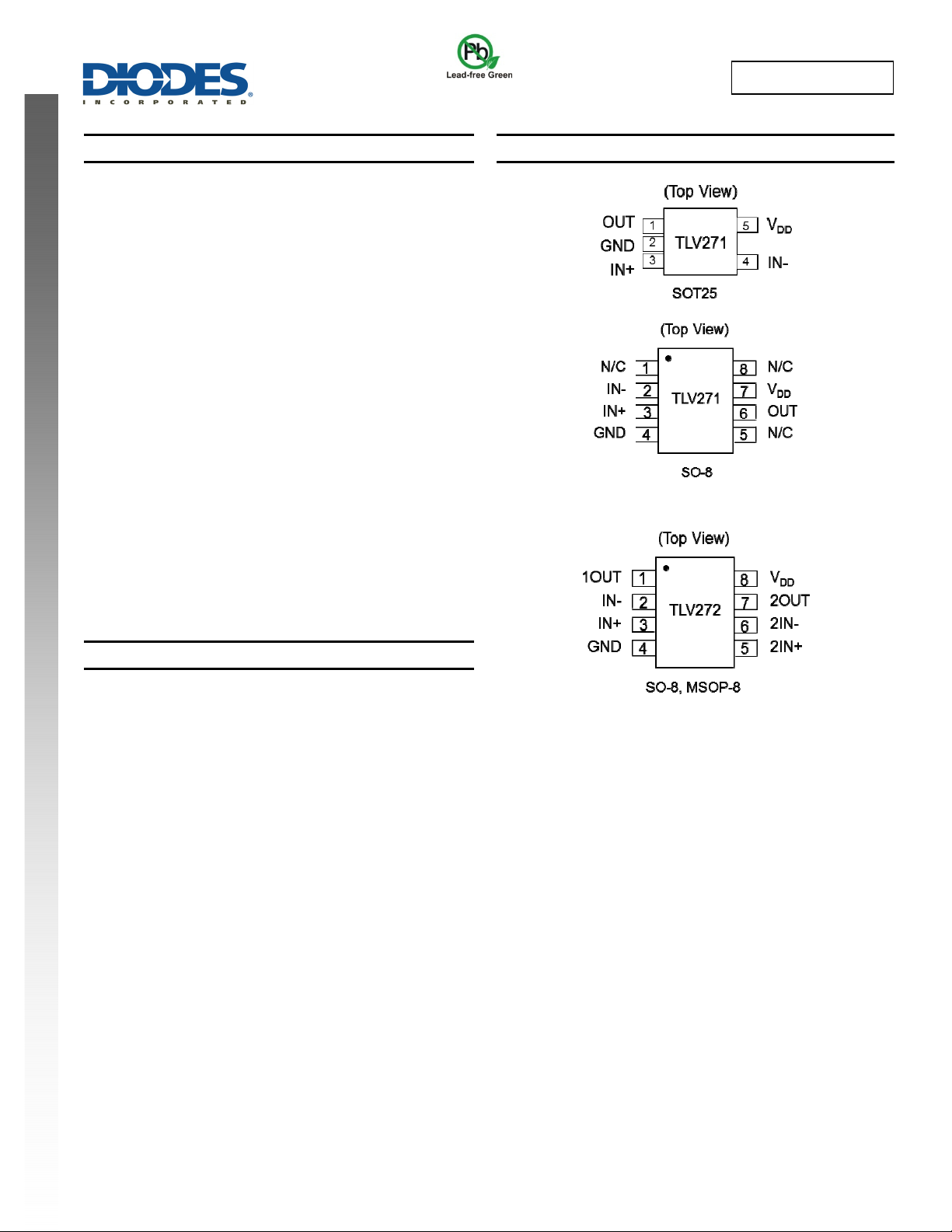
Pin Assignments
(Future Product)
Features
• High performance alternative to TLC27x series
• Rail to rail output
• Wide bandwidth: 2MHz
• High slew rate: 2.0 V/µs
• Wide range of supply voltages: 2.7V to 16V
• Low supply current: 550µA per channel
• Low input noise voltage: 35nV/√Hz
• Low input bias current: 1pA
• Specified temperature ranges:
0°C to +70°C: commercial grade
-40°C to +125°C: industrial grade
• Totally Lead-Free & Fully RoHS Compliant (Notes 1 & 2)
• Halogen and Antimony Free. “Green” Device (Note 3)
Notes: 1. No purposely added lead. Fully EU Directive 2002/95/EC (RoHS) & 2011/65/EU (RoHS 2) compliant.
2. See http://www.diodes.com/quality/lead_free.html for more information about Diodes Incorporated’s definitions of Halogen- and Antimony-free, "Green"
and Lead-free.
3. Halogen- and Antimony-free "Green” products are defined as those which contain <900ppm bromine, <900ppm chlorine (<1500ppm total Br + Cl) and
<1000ppm antimony compounds.
(Future Product)
TLV271/ TLV272
Document number: DS35394 Rev. 4 - 2
1 of 17
www.diodes.com
December 2013
© Diodes Incorporated
Page 2
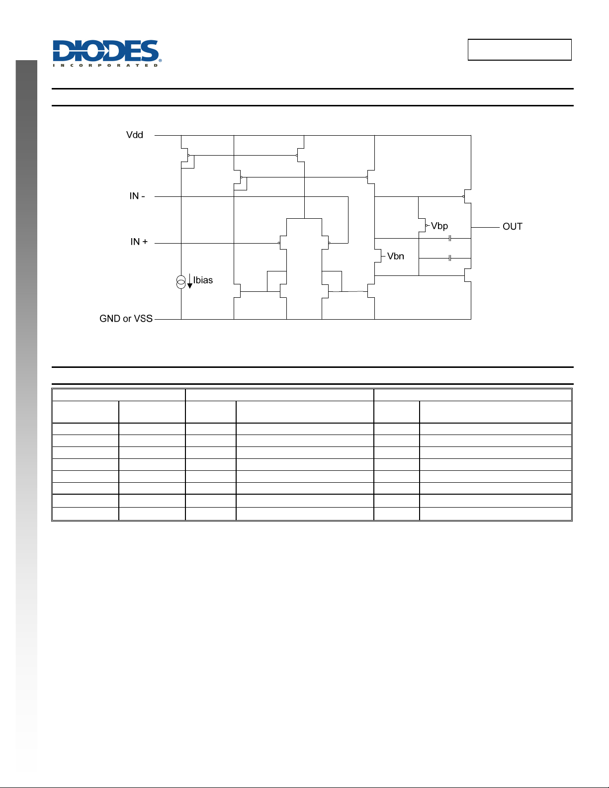
Simplified Schematic Diagram
TLV271/TLV272
NEW PRODUCT
Pin Descriptions
Pin Number TLV271 TLV272
SOT25
1 N/C No connection 1OUT Output op-amp 1
4 2 IN- Inverting input 1IN- Inverting input op-amp 1
3 3 IN+ Non-inverting input 1IN+ Non-inverting input op-amp 1
2 4 GND Ground GND Ground
5 N/C No connection 2IN+ Non inverting input op-amp 2
1 6 OUT Output 2IN- Inverting input op-amp 2
5 7
8 N/C
SO-8/
MSOP-8
Pin
Name
V
DD
Supply
No connection
Function
Pin
Name
2OUT Output op-amp 2
V
DD
Supply
Function
TLV271/ TLV272
Document number: DS35394 Rev. 4 - 2
2 of 17
www.diodes.com
December 2013
© Diodes Incorporated
Page 3
TLV271/TLV272
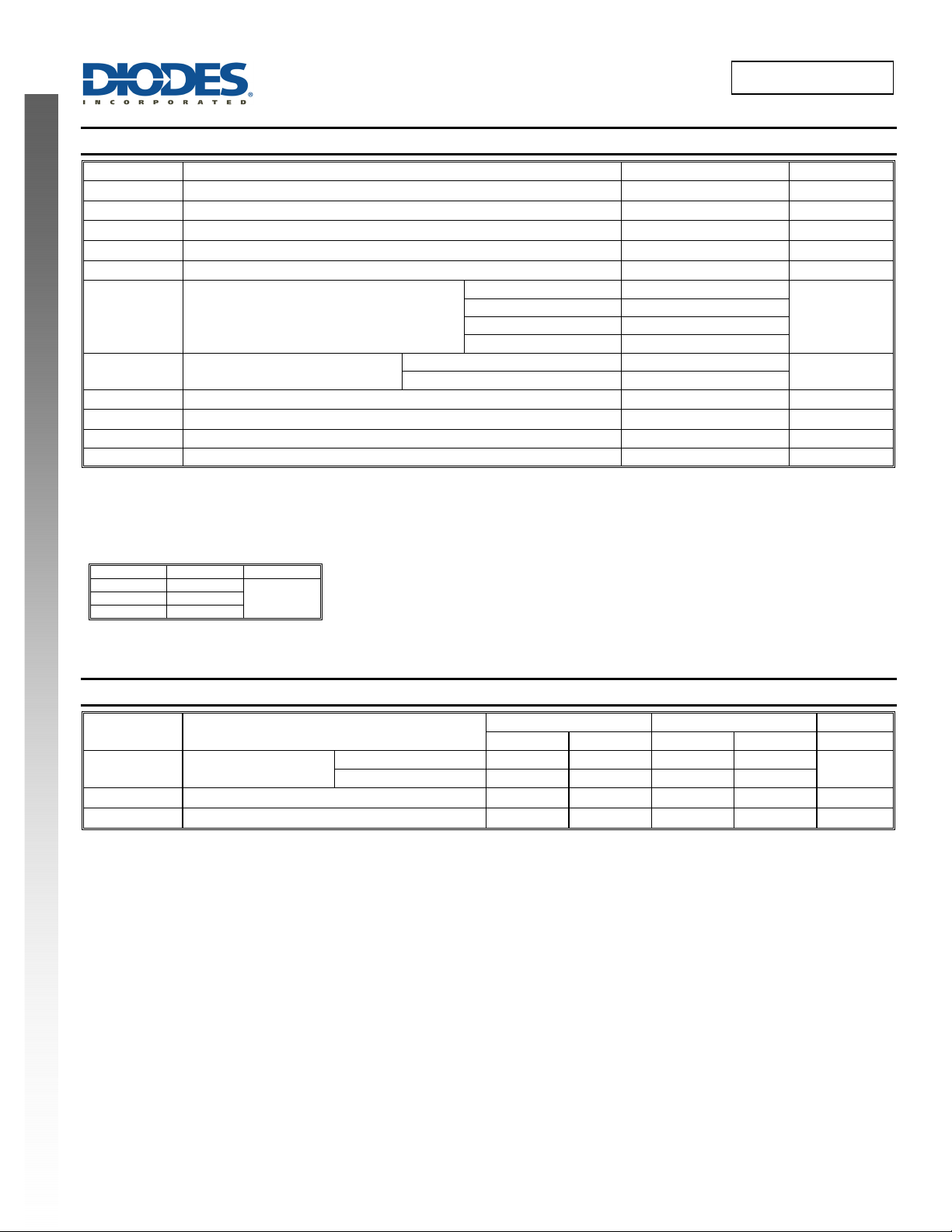
Absolute Maximum Ratings (Note 4)
Symbol Parameter Rating Unit
VDD
VID
VIN
IIN
IO
PD
TA
TJ
TST
ESD HBM Human Body Model ESD Protection (1.5kΩ in series with 100pF) 2 kV
ESD MM Machine Model ESD Protection 150 V
NEW PRODUCT
Notes: 4. Stresses beyond those listed under absolute maximum ratings may cause permanent damage to the device. These are stress ratings only; functional
Package θJA Unit
SOT25 180
SO-8 150
MSOP-8 155
Supply Voltage: (Note 5) 16.5 V
Differential Input Voltage
Input Voltage Range (Note 5)
Input Current Range ±10 mA
Output Current Range ±100 mA
TLV271 SOT25 220 mW
Power Dissipation (Note 6)
Operating Temperature Range
Operating Junction Temperature 150 °C
Storage Temperature Range -65 to +150 °C
operation of the device at these or any other conditions beyond those indicated under recommended operating conditions is not implied. Exposure to
absolute-maximum-rated conditions for extended periods may affect device reliability.
5. All voltage values, except differential voltages, are with respect to ground
6. For operating at high temperatures, the TLV27x must be derated to zero based on a +150°C maximum junction temperature and a thermal resistance
as below when the device is soldered to a printed circuit board, operating in a still air ambient:
°C/W
C grade 0 to +70
I grade -40 to +125
TLV271 SO-8 396 mW
TLV272 SO-8 396 mW
TLV272 MSOP-8 300 mW
±VDD
-0.2 to V
DD
+0.2V
Recommended Operating Conditions
V
V
mW
°C
Symbol Parameter
VDD
VIC
TA
Supply Voltage
Common Mode Input Voltage
Operating Free Air Temperature
Single Supply 2.7 16 2.7 16 V
Split Supply ±1.35 ±8 ±1.35 ±8
Min Max Min Max
C grade I grade Unit
0
0 +70 -40 +125 °C
V
-1.35
DD
0
V
-1.35
DD
V
TLV271/ TLV272
Document number: DS35394 Rev. 4 - 2
3 of 17
www.diodes.com
December 2013
© Diodes Incorporated
Page 4
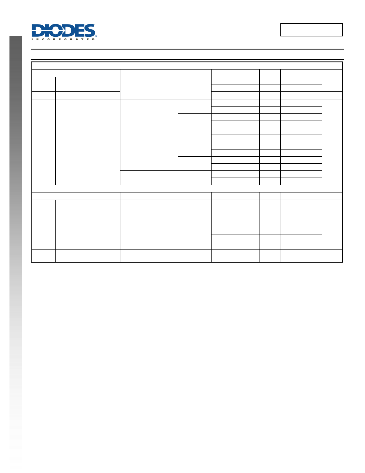
Electrical Characteristics (@T
DC Performance
Parameter Conditions
Input Offset Voltage
VIO
Offset Voltage Drift +25°C —
α
VIO
Large Signal Differential
AVD
Voltage Gain
CMRR
Common Mode Rejection
Ratio
NEW PRODUCT
Input Characteristics
Parameter Conditions
Input Offset Current
IIO
Input Bias Current
IIB
Differential Input Resistance — +25°C
r
i(d)
Common Mode Input
CIC
Capacitance
= +25°C and VDD = 2.7V, 5V, ±5V unless otherwise specified.)
A
= VDD/2, VO = VDD/2,
V
IC
= 50Ω, RL = 10kΩ
R
S
V
= VDD/2, RL = 10kΩ
O(PP)
= 0 to V
V
IC
= 50Ω
R
S
VIC = -5 to V
= 50Ω
R
S
= 5V, VIC = VDD/2,
V
DD
= VDD/2, RS = 50Ω
V
O
-1.35V,
DD
DD
-1.35V,
f = 21kHz +25°C
V
= 2.7V
DD
VDD = 5V
VDD = ±5V
= 2.7V
V
DD
VDD = 5V
V
= ±5V
DD
TLV271/TLV272
T
A
+25°C — 0.5 5
-40°C to +125°C — — 7
+25°C 97 106 —
-40°C to +125°C 76 — —
+25°C 100 110 —
-40°C to +125°C 86 — —
+25°C 100 115 —
-40°C to +125°C 90 — —
+25°C 58 70 —
-40°C to +125°C 55 — —
+25°C 65 80 —
-40°C to +125°C 62 — —
+25°C 69 85 —
-40°C to +125°C 66
T
A
+25°C — 1 60
+70°C — — 100
+125°C — — 1000
+25°C — 1 60
+70°C — — 100
+125°C — — 1000
Min Typ Max Unit
6 —
— —
Min Typ Max Unit
— 100 —
— 12 —
mV
µV/°C
dB
dB
pA
MΩ
pF
TLV271/ TLV272
Document number: DS35394 Rev. 4 - 2
4 of 17
www.diodes.com
December 2013
© Diodes Incorporated
Page 5
Electrical Characteristics (cont.) (@T
Output Characteristics
Parameter Conditions
V
I
OH
High Level Output Voltage
VOH
VIC = VDD/2,
I
OH
NEW PRODUCT
Low Level Output Voltage
VOL
Output Current
IO
Power Supply
Parameter Conditions
Supply Current (per op-amp)
IDD
Power Supply Rejection Ratio
IIB
(∆V
/∆VIO)
DD
V
I
OL
VIC = VDD/2,
I
OL
V
V
VO = 0.5V from rail,
V
VO = 0.5V from rail,
V
VO = VDD/2
V
V
= +25°C and VDD = 2.7V, 5V, ±5V unless otherwise specified.)
A
= VDD/2,
IC
= -1mA
= -5mA
= VDD/2,
IC
= 1mA
= 5mA
= 0.5V from rail,
O
= 2.7V
DD
= 5V
DD
= 10V
DD
= 2.7V to 16V,
DD
= VDD/2, No load
IC
TLV271/TLV272
T
A
= 2.7V
V
DD
VDD = 5V
VDD = ±5V
= 2.7V
V
DD
VDD = 5V
VDD = ±5V
= 2.7V
V
DD
VDD = 5V
VDD = ±5V
= 2.7V
V
DD
VDD = 5V
VDD = ±5V
+25°C 2.55 2.58 —
-40°C to +125°C 2.48 — —
+25°C 4.9 4.93 —
-40°C to +125°C 4.85 — —
+25°C 4.92 4.96 —
-40°C to +125°C 4.9 — —
+25°C 1.9 2.1 —
-40°C to +125°C 1.5 — —
+25°C 4.6 4.68 —
-40°C to +125°C 4.5 — —
+25°C 4.7 4.84 —
-40°C to +125°C 4.65 — —
+25°C — 0.1 0.15
-40°C to +125°C — — 0.22
+25°C — 0.05 0.1
-40°C to +125°C — — 0.15
+25°C — -4.95 -4.92
-40°C to +125°C — — -4.9
+25°C — 0.5 0.7
-40°C to +125°C — — 1.1
+25°C — 0.28 0.4
-40°C to +125°C — — 0.5
+25°C — -4.84 -4.7
-40°C to +125°C — — -4.65
Positive rail +25°C — 4 —
Negative rail +25°C
Positive rail +25°C — 7 —
Negative rail +25°C
Positive rail +25°C — 13 —
Negative rail +25°C
T
A
V
= 2.7V
DD
VDD = 5V
VDD = 10V
+25°C
+25°C
+25°C — 625 800
-40°C to +125°C — — 1000
+25°C 70 80 —
-40°C to +125°C
Min Typ Max Unit
— 5 —
— 8 —
— 12 —
Min Typ Max Unit
— 470 560
— 550 660
65
— —
V
V
mA
µA
dB
TLV271/ TLV272
Document number: DS35394 Rev. 4 - 2
5 of 17
www.diodes.com
December 2013
© Diodes Incorporated
Page 6
Electrical Characteristics (cont.) (@T
Dynamic Performance
Parameter Conditions
UGBW Unity Gain Bandwidth
SR Slew Rate At Unity Gain
Phase Margin
Φm
Gain Margin
NEW PRODUCT
tS
Settling Time
Noise/Distortion Performance
Parameter Conditions
THD+N
Total Harmonic Distortion Plus
Noise
Equivalent Input Noise Voltage
Vn
Equivalent Input Noise Current
In
TLV271/ TLV272
Document number: DS35394 Rev. 4 - 2
TLV271/TLV272
= +25°C and VDD = 2.7V, 5V, ±5V unless otherwise specified.)
A
T
A
R
= 2kΩ,
L
= 10pF
C
L
= VDD/2,
V
O(PP)
= 50pF,
C
L
R
= 10kΩ
L
RL = 2kΩ, CL = 10pF
R
= 2kΩ, CL = 10pF
L
= 2.7V,
V
DD
V
A
R
= 1V,
(STEP)PP
= -1, CL = 10pF,
V
= 2kΩ
L
= 2.7V
V
DD
VDD = 5V to
10V
V
= 2.7V
DD
VDD = 5V
VDD = 10V
0.1%
+25°C — 1.7 —
+25°C
+25°C 1.2 2.1 —
-40°C to +125°C 1 — —
+25°C 1.25 2.0 —
-40°C to +125°C 1.05 — —
+25°C 1.3 2.2 —
-40°C to +125°C 1.1 — —
+25°C
+25°C
+25°C
VDD = 5V, ±5V
V
A
R
V
V
R
VDD = 5V, ±5V
V
R
= 1V,
(STEP)PP
= -1, CL = 47pF,
V
= 2kΩ
L
= 2.7V,
DD
= VDD/2,
O(PP)
= 2kΩ, f = 10kHz
L
= VDD/2,
O(PP)
= 2kΩ, f = 10kHz
L
0.1% +25°C — 2 —
T
A
= 1
A
V
AV = 10
AV = 100
= 1
A
V
AV = 10
AV = 100
+25°C
+25°C
+25°C
+25°C
+25°C
+25°C
f = 1kHz +25°C — 35 —
f = 10kHz +25°C — 25 —
f = 1kHz
+25°C
6 of 17
www.diodes.com
Min Typ Max Unit
— 1.9 —
— 65°C —
— 12 — dB
— 2.9 —
Min Typ Max Unit
— 0.02 —
— 0.05 —
— 0.18 —
— 0.02 —
— 0.09 —
— 0.5 —
nV/√Hz
—
0.6 —
December 2013
© Diodes Incorporated
MHz
V/µs
—
µs
%
fA/√Hz
Page 7

Typical Performance Characteristics
List of Figures
Input Offset Voltage
Input Bias Current, Input Offset Current
Supply Current
High Level Output Voltage
Low Level Output Voltage
Differential Voltage Gain And Phase
Phase Margin
Equivalent Input Noise Voltage
Peak To Peak Output Voltage
NEW PRODUCT
VIO
IIB,IIO
IDD
PSRR Power Supply Rejection Ratio
CMRR Common Mode Rejection Ratio
VOH
VOL
SR Slew Rate
A
Φ
VD,
Φm
— Gain Bandwidth Product vs. free air temperature 18
Vn
V
O(PP)
— Voltage Follower Large Signal Pulse Response — 21, 22
— Voltage Follower Small Signal Pulse Response — 23
— Inverting Large Signal Response — 24, 25
— Inverting Small Signal Response — 26
— Crosstalk vs. frequency 27
TLV271/ TLV272
Document number: DS35394 Rev. 4 - 2
TLV271/TLV272
Figure
vs. free air temperature
vs. free air temperature
vs. supply voltage
vs. frequency 4
vs. free air temperature 5
vs. frequency 6
vs. free air temperature 7
vs. high level output current
vs. high level output current
vs. free air temperature 14
vs. supply voltage 15
vs. frequency
vs. capacitive load
vs. frequency
vs. frequency
7 of 17
www.diodes.com
1
2
3
8, 9, 10
11,12,13
16
17
19
20
December 2013
© Diodes Incorporated
Page 8

P
U
T OFF
T
OLTAG
UPPLY CUR
RENT
PSR
R-P
OWER SUPPLY R
C
TION RATIO
P
R
R
P
O
R SU
P
PLY R
C
T
O
R
TIO
C
R
R
C
O
O
O
R
C
TION RAT
O
Typical Performance Characteristics (cont.)
0
V = +2.7V
DD
V = 5VDD±
300.0
270.0
240.0
V =5V, V = V/2
DD IC DD
V = V /2, R = 50
ODD S
Ω
TLV271/TLV272
NEW PRODUCT
E (mV)
-1
V
SE
-2
IN
-3
-50 -25 0 25 50 75
TEMPERATURE (°C)
Figure 1 Input Offset Voltage vs. Temperature
500
450
400
350
(µA)
300
T = +70
A
T = 0
A
250
200
T = -40
A
V = +5V
DD
100 125
T = +125
A
T = +25
A
210.0
180.0
I
IB
150.0
120.0
90.0
INPUT BIAS CURRENT (pA)
I
IO
60.0
30.0
0.0
-50 -25 0 25 50 75 100 125
TEMPERATURE (°C)
Figure 2 Input Bias and Offset Current vs. Temperature
100
V = 10V
DD
(dB)
80
V = 2.7V
DD
60
EJE
V = 5V
DD
40
150
S
100
# 1, A = 1
50
0
0246810121416
V
V = V /2
IC DD
SUPPLY VOLTAGE (V)
Figure 3 Supply Current vs. Supply Voltage
120
(dB)
110
A
V = 2.7V to 16V
DD
20
0
10 100 1000 10000 100000 1000000
FREQUENCY (Hz)
Figure 4 Power Supply Rejection Ratio vs. Frequency
120
(dB)
I
100
N
I
100
EJE
90
80
WE
70
-
S
60
-50-25 0 255075100125
TEMPERATURE (°C)
Figure 5 Power Supply Rejection Ratio vs. Temperature
TLV271/ TLV272
Document number: DS35394 Rev. 4 - 2
8 of 17
www.diodes.com
80
±
1.35
EJE
60
DE
±
N M
40
5
MM
20
-
M
0
10 100 1000 10000
100000 1000000
FREQUENCY (Hz)
Figure 6 Common Mode Rejection Ratio vs. Frequency
±
2.5
December 2013
© Diodes Incorporated
Page 9

CMR
R
C
OMM
ON M
O
E R
EJE
CTION R
A
O
G
O
O
G
O
O
G
O
O
G
O
EVEL O
UTP
U
O
A
E
O
O
U
TPU
T VO
TAG
Typical Performance Characteristics (cont.)
120
(dB)
V = 2.7V
DD
V = 5VDD±
°
NEW PRODUCT
TI
100
V = 5V
DD
80
60
D
40
20
-
0
-50 -25 0 25 50 75 100 125
TEMPERATURE ( C)
Figure 7 Common Mode Re jection Ratio vs. Temperaure
5.0
TLV271/TLV272
2.8
2.4
E (V)
2.0
LTA
1.6
UTPUT V
1.2
0.8
T = +70CA°
T = +105 CA°
H-LEVEL
HI
0.4
0.0
T = +125 CA°
V = 2.7V
DD
048121620
HIGH-LEVEL OUTPUT CURRENT (mA)
Figure 8 High-Level Output Voltage vs.
High-Level Output Current
10.0
T = +25CA°
T = 0CA°
T = -40CA°
4.5
4.0
3.5
LTAGE (V)
3.0
2.5
UTPUT V
2.0
T = +70CA°
1.5
V = 5V
DD
T = +105CA°
T = +125 CA°
1.0
HIGH-LEVEL
0.5
0.0
01224364860
T = +25CA°
T = 0CA°
T = -40CA°
HIGH-LEVEL OUTPUT CURRENT (mA)
Figure 9 High-Level Output Voltage vs.
High-Level Output Current
2.8
V = 2.7V
DD
2.4
T = +125CA°
(V)
T = +25CA°
G
2.0
LT
T V
1.6
T = +105 CA°
T = +70CA°
T = 0CA°
T = -40CA°
1.2
0.8
W-L
L
0.4
0.0
0 4 8 1216 20 2428 3236 40
LOW-LEVEL OUTPUT CURRENT (mA)
Figure 11 Low-Level Output Voltage vs.
Low-Level Output Current
8.0
E (V)
LTA
6.0
T = +25CA°
UTPUT V
4.0
H-LEVEL
2.0
HI
0.0
020406080100120
V = 10V
DD
T = +70CA°
T = 0CA°
T = +105 CA°
T = -40CA°
T = +125CA°
HIGH-LEVEL OUTPUT CURRENT (mA)
Figure 10 High-Level Output Voltage vs.
High-Level Output Current
5.0
V = 5V
DD
4.5
4.0
E (V)
3.5
L
T = +125CA°
T = +105CA°
3.0
2.5
2.0
T = +70CA°
T = +25CA°
1.5
W-L EV EL
1.0
L
0.5
0.0
0 102030405060708090
T = -40CA°
T = 0CA°
LOW-LEVEL OUTPUT CURRENT (mA)
Figure 12 Low-Level Output Voltage vs.
Low-Level Output Current
TLV271/ TLV272
Document number: DS35394 Rev. 4 - 2
9 of 17
www.diodes.com
December 2013
© Diodes Incorporated
Page 10

O
OUT
P
U
T
OLTAG
R
RAT
D
DIF
FEREN
T
OLTAGE GAIN
P
A
SE M
A
R
GBMP
G
T
H P
R
ODUCT
H
Typical Performance Characteristics (cont.)
10.0
V = 10V
DD
T = +125 CA°
T = +105 CA°
T = +70CA°
T = 0CA°
T = -40CA°
Low-Level Output Current
NEW PRODUCT
8.0
E (V)
6.0
V
4.0
W-LEVEL
2.0
L
0.0
0 20 40 60 80 100 120 140
LOW-LEVEL OUTPUT CURRENT (mA)
Figure 13 Low-Level Output Voltage vs.
2.5
T = +25CA°
TLV271/TLV272
3
2.5
SR-
2
SR+
ATE (V/ µs)
1.5
1
SLEW
0.5
V = 5V, A = 1, R = 10k,
DD V L
C = 50pF, V =V /2
L O(PP) DD
0
-50-25 0 255075100125
120
TEMPERATURE (°C)
Figure 14 Slew Rate vs. Temperature
180
2
SR+
1.5
E (V/µs)
SR-
1
SLEW
0.5
0
2.5 5 7.5 10 12.5 15
SUPPLY VOLTAGE (V)
Figure 15 Slew Rate vs. Supply Voltage
100
90
80
0
Ω
50
Ω
70
60
GIN (°)
100
Ω
50
100
(dB)
80
60
40
IAL V
20
0
-
-20
135
90
45
0
-45
-90
-135
PHASE (°)
AV
-40
10 1000 100000 10000000
-180
FREQUENCY (Hz)
Figure 16 Differential Voltage Gain and Phase vs. Frequency
3.0
z)
2.5
(M
V = 2.5VDD±
V = 5VDD±
2.0
1.5
V = 1.35VDD±
40
H
30
20
1.0
AIN BANDWID
-
0.5
10
0
10 100 1000
C , CAPACITIVE LOAD (pF)
L
Figure 17 Phase Margin vs. Capacitive Load
0.0
-40 -25 -10 5 20 35 50 65 80 95 110 125
T , FREE-AIR TEMPERATURE (°C)
A
Figure 18 Gain Bandwidth Product vs. Free Air Temperature
TLV271/ TLV272
Document number: DS35394 Rev. 4 - 2
10 of 17
www.diodes.com
December 2013
© Diodes Incorporated
Page 11

P
P
OUTPU
T VO
T
G
Typical Performance Characteristics (cont.)
220
5V
200
180
10V
160
140
2.7V
120
100
80
60
40
20
0
10 100 1000 10000 100000
FREQUENCY (Hz)
Figure 19 Equivalent Input Noise Voltage vs. Frequency
NEW PRODUCT
√
N
V -EQUIVALENT INPUT NOISE VOLTAGE (nv Hz)
TLV271/TLV272
11
V = 10V
DD
10
E (V)
9
A
L
8
7
6
V = 5V
DD
5
EAK
4
3
EAK-to-
2
1
O(PP)
V,
0
10 1000 100000 10000000
Figure 20 Peak-to-Peak Output Voltage vs. Frequency
V = 2.7V
DD
FREQUENCY (Hz)
V = 5V, A = 1, V = 3V , R = 2K, C = 10pF
DD V I PP L L
Figure 21 Voltage Follower Large
Signal Pulse Response V = 5V
V = 5V, A = 1, V = 100mV , R = 2K, C = 10pF
DD V I PP L L
DD
V = 10V, A = 1, V = 6V , R = 2K, C = 10pF
DD V I PP L L
Figure 22 Voltage Follower Large
Signal Pulse Response V = 10V
V = 5V, A = 1, V = 3V
DD V I PP
DD
Figure 23 Voltage Follower Small Signal Pulse Response
Figure 24 Inverting Large Signal Pulse Response V = 5V
DD
TLV271/ TLV272
Document number: DS35394 Rev. 4 - 2
11 of 17
www.diodes.com
December 2013
© Diodes Incorporated
Page 12

CROSST
Typical Performance Characteristics (cont.)
TLV271/TLV272
NEW PRODUCT
V = 10V, A = 1, V = 6V
DD V I PP
Figure 25 Inverting Large Signal Pulse Response V = 10V
0
-20
-40
-60
ALK (dB)
-80
DD
V = 5V, A = 1, V = 100mV
DD V I PP
Figure 26 Inverting Small Signal Pulse Response
-100
-120
-140
-160
10 100 1000 10000 100000
Figure 27 Crosstalk vs. Frequency TLV272
TLV271/ TLV272
Document number: DS35394 Rev. 4 - 2
FREQUENCY (Hz)
12 of 17
www.diodes.com
December 2013
© Diodes Incorporated
Page 13

TLV271/TLV272
Application Information
Driving a Capacitive Load
When the amplifier is configured as below, capacitive loading directly on the output can decrease the device’s phase margin leading to high
frequency ringing or oscillations. Therefore, for capacitive loads of greater than 100pF, it is recommended that a resistor be placed in series (R
with the output of the amplifier, as shown in Figure 25. A minimum value of 20Ω should work well for most applications.
NULL
)
Figure 28 Driving a Capacitive Load
Offset Voltage
NEW PRODUCT
The output offset voltage, (VOO) is the sum of the input offset voltage (VIO) and both input bias currents (IIB) times the corresponding gains. The
following schematic and formula can be used to calculate the output offset voltage:
Figure 29 Output Offset Voltage Model
Other Configurations
When receiving low-level signals, limiting the bandwidth of the incoming signals into the system is often required. The simplest way to accomplish
this is to place an RC filter at the non-inverting terminal of the amplifier (see Figure 30).
Figure 30. Single Pole Low Pass Filter
If even more attenuation is needed, a multiple pole filter is required. The Sallen-Key filter can be used for this task. For best results, the amplifier
should have a bandwidth that is 8 to 10 times the filter frequency bandwidth. Failure to do this can result in phase shift of the amplifier.
Figure 31. 2-Pole Low-Pass Sallen-Key Filter
TLV271/ TLV272
Document number: DS35394 Rev. 4 - 2
13 of 17
www.diodes.com
December 2013
© Diodes Incorporated
Page 14

Ordering Information
TLVC27XXXX
TLV271/TLV272
-
X
Number of
Op - Amps
1 : Single
:
2
Dual
Temperaure
Grade
C:Commercial
: Industrial
Package
W5 : SOT25
S:SO-8
Packing
7 : Tape & 7" Reel
13 : Tape & 13" ReelI
MSOP8:M8
Part Number Package Code
TLV271CW5-7 W5 0 to +70°C SOT25 3000/Tape & Reel -7
TLV271CS-13** S 0 to +70°C SO-8 2500/Tape & Reel -13
NEW PRODUCT
TLV271IW5-7 W5 -40°C to +125°C SOT25 3000/Tape & Reel -7
TLV271IS-13** S -40°C to +125°C SO-8 2500/Tape & Reel -13
TLV272CS-13** S 0 to +70°C SO-8 2500/Tape & Reel -13
TLV272CM8-13** M8 0 to +70°C MSOP-8 2500/Tape & Reel -13
TLV272IS-13** S -40°C to +125°C SO-8 2500/Tape & Reel -13
TLV272IM8-13** M8 -40°C to +125°C MSOP-8 2500/Tape & Reel -13
**Future Products
Operating
Temperature Range
Packaging
Quantity Part Number Suffix
7” or 13” Tape and Reel
Marking Information
SOT25
Part mark Part number
BV TLV271CW5
BW TLV271IW5
SO-8
Part mark Part number
V271C TLV271CS
V271I TLV271IS
V272C TLV272CS
MSOP-8
TLV271/ TLV272
Document number: DS35394 Rev. 4 - 2
V272I TLV272IS
Part mark Part number
V272C TLV272CM8
V272I TLV272IM8
14 of 17
www.diodes.com
December 2013
© Diodes Incorporated
Page 15

Package Outline Dimensions (All dimensions in mm.)
Please see AP02002 at http://www.diodes.com/datasheets/ap02002.pdf for latest version.
SOT25
NEW PRODUCT
SO-8
K
J
A
B C
H
N
D
L
M
e
b
D
E1
A2
E
A1
Detail ‘A’
h
°
45
A3
A
L
0.254
Gauge Plane
Seating Plane
7°~9
°
MSOP-8
D
x
y
1
A2
e
A1
E
b
TLV271/ TLV272
Document number: DS35394 Rev. 4 - 2
0.25
Gauge Plane
Seating Plane
A3
A
4
x
1
Detail C
E3
E1
0
°
4
x
1
0
°
L
See Detail C
a
c
15 of 17
www.diodes.com
Detail ‘A’
Dim Min Max Typ
SOT25
A 0.35 0.50 0.38
B 1.50 1.70 1.60
C 2.70 3.00 2.80
D
⎯ ⎯
H 2.90 3.10 3.00
J 0.013 0.10 0.05
K 1.00 1.30 1.10
L 0.35 0.55 0.40
M 0.10 0.20 0.15
N 0.70 0.80 0.75
0° 8°
α
All Dimensions in mm
Dim Min Max
Dim Min Max Typ
A - 1.10 A1 0.05 0.15 0.10
A2 0.75 0.95 0.86
A3 0.29 0.49 0.39
b 0.22 0.38 0.30
c 0.08 0.23 0.15
D 2.90 3.10 3.00
E 4.70 5.10 4.90
E1 2.90 3.10 3.00
E3 2.85 3.05 2.95
e - - 0.65
L 0.40 0.80 0.60
a 0° 8° 4°
x - - 0.750
y - - 0.750
All Dimensions in mm
SO-8
A - 1.75
A1 0.10 0.20
A2 1.30 1.50
A3 0.15 0.25
b 0.3 0.5
D 4.85 4.95
E 5.90 6.10
E1 3.85 3.95
e 1.27 Typ
h - 0.35
L 0.62 0.82
0° 8°
θ
All Dimensions in mm
MSOP-8
0.95
⎯
TLV271/TLV272
December 2013
© Diodes Incorporated
Page 16

Suggested Pad Layout
Please see AP02001 at http://www.diodes.com/datasheets/ap02001.pdf for the latest version.
SOT25
C2C2
C1
NEW PRODUCT
SO-8
G
Z
Y
X
X
MSOP-8
C2
Y
X C
C1
Y1
TLV271/ TLV272
Document number: DS35394 Rev. 4 - 2
Y
16 of 17
www.diodes.com
Dimensions Value (in mm)
Z
G
X
Y
C1 2.40
C2
Dimensions Value (in mm)
X 0.60
Y 1.55
C1 5.4
C2 1.27
Dimensions Value (in mm)
C 0.650
X 0.450
Y 1.350
Y1 5.300
3.20
1.60
0.55
0.80
0.95
TLV271/TLV272
December 2013
© Diodes Incorporated
Page 17

TLV271/TLV272
DIODES INCORPORATED MAKES NO WARRANTY OF ANY KIND, EXPRESS OR IMPLIED, WITH REGARDS TO THIS DOCUMENT,
INCLUDING, BUT NOT LIMITED TO, THE IMPLIED WARRANTIES OF MERCHANTABILITY AND FITNESS FOR A PARTICULAR PURPOSE
(AND THEIR EQUIVALENTS UNDER THE LAWS OF ANY JURISDICTION).
Diodes Incorporated and its subsidiaries reserve the right to make modifications, enhancements, improvements, corrections or other changes
without further notice to this document and any product described herein. Diodes Incorporated does not assume any liability arising out of the
application or use of this document or any product described herein; neither does Diodes Incorporated convey any license under its patent or
trademark rights, nor the rights of others. Any Customer or user of this document or products described herein in such applications shall assume
all risks of such use and will agree to hold Diodes Incorporated and all the companies whose products are represented on Diodes Incorporated
website, harmless against all damages.
Diodes Incorporated does not warrant or accept any liability whatsoever in respect of any products purchased through unauthorized sales channel.
Should Customers purchase or use Diodes Incorporated products for any unintended or unauthorized application, Customers shall indemnify and
hold Diodes Incorporated and its representatives harmless against all claims, damages, expenses, and attorney fees arising out of, directly or
indirectly, any claim of personal injury or death associated with such unintended or unauthorized application.
Products described herein may be covered by one or more United States, international or foreign patents pending. Product names and markings
noted herein may also be covered by one or more United States, international or foreign trademarks.
This document is written in English but may be translated into multiple languages for reference. Only the English version of this document is the
final and determinative format released by Diodes Incorporated.
NEW PRODUCT
Diodes Incorporated products are specifically not authorized for use as critical components in life support devices or systems without the express
written approval of the Chief Executive Officer of Diodes Incorporated. As used herein:
A. Life support devices or systems are devices or systems which:
1. are intended to implant into the body, or
labeling can be reasonably expected to result in significant injury to the user.
B. A critical component is any component in a life support device or system whose failure to perform can be reasonably expected to cause the
failure of the life support device or to affect its safety or effectiveness.
Customers represent that they have all necessary expertise in the safety and regulatory ramifications of their life support devices or systems, and
acknowledge and agree that they are solely responsible for all legal, regulatory and safety-related requirements concerning their products and any
use of Diodes Incorporated products in such safety-critical, life support devices or systems, notwithstanding any devices- or systems-related
information or support that may be provided by Diodes Incorporated. Further, Customers must fully indemnify Diodes Incorporated and its
representatives against any damages arising out of the use of Diodes Incorporated products in such safety-critical, life support devices or systems.
Copyright © 2013, Diodes Incorporated
www.diodes.com
2. support or sustain life and whose failure to perform when properly used in accordance with instructions for use provided in the
IMPORTANT NOTICE
LIFE SUPPORT
TLV271/ TLV272
Document number: DS35394 Rev. 4 - 2
17 of 17
www.diodes.com
December 2013
© Diodes Incorporated
 Loading...