

Page 1
5
3
Description
TL431/TL432
ADJUSTABLE PRECISION SHUNT REGULATOR
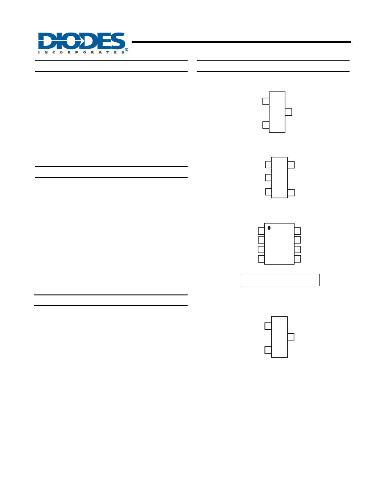
Pin Assignments
The TL431 and TL432 are three terminal adjustabl e shunt
regulators offering excellent temperature stability and output
current handling capability up to 100mA. The output voltage
may be set to any chosen voltage between 2.5 and 36 volt s
by selection of two external divider resistors.
The devices can be used as a replacement for zener diodes
in many applications requiring an improvement in zener
performance. Diodes’ TL431 has the same electrical
specifications as the industry standard ‘431 and is available
in 2 grades with initial tolerances of 1% and 0.5% for the
A and B grades respectively.
Features
• Temperature range -40 to +125ºC
• Reference Voltage Tolerance at 25°C
• TL431A: 2.495V ± 1.0%
• TL431B: 2.495V ± 0.5%
• Low Output Noise
• 0.2Ω Typical Output Impedance
• Sink Current Capability: 1mA to 100mA
• Adjustable Output Voltage: V
• All devices are:
• Totally Lead-Free & Fully RoHS compliant
(Notes 1 & 2)
• Halogen and Antimony Free. “Green” Device
(Note 3)
REF
to 36V
Applications
• Opto-Coupler Linearisers
• Shunt Regulators
• Improved Zener
• Variable Reference
CATHODE
REF
NC
Leave floating or
connect to pin 5
CATHODE
CATHODE
ANODE
ANODE
NC
SO-8 is a future product
REF
CATHODE
TL431
(Top View)
1
2
SOT23
(Top View)
2
3
SOT2
(Top View)
1
2
3
4
SO-8
TL432
(Top View)
1
2
ANODE
3
5
4
3
ANODE
REF
REF
8
ANODE
7
6
ANODE
5
NC
ANODE
SOT2
Notes: 1. No purposely added lead. Fully EU Directive 2002/95/EC (RoHS) & 2011/65/EU (RoHS 2) compliant.
2. See http://www.diodes.com/quality/lead_free.html for more information about Diodes Incorporated’s definitions of Halogen and Antimony free,
"Green" and Lead-Free.
3. Halogen and Antimony free "Green” products are defined as those which contain <900ppm bromine, <900ppm chlorine (<1500ppm total Br + Cl) and
<1000ppm antimony compounds.
TL431 *SO-8 is a future package
Document number: DS35044 Rev. 6 - 2
1 of 14
www.diodes.com
April 2012
© Diodes Incorporated
Page 2
TL431/TL432
Absolute Maximum Ratings (Note 4)
Symbol Parameter Rating Unit
VKA
IKA
I
REF
TJ
TST
PD
Notes: 4. Operation above the absolute maximum rating may cause device failure. Operation at the absolute maximum ratings, for extended periods, may
reduce device reliability. Unless otherwise stated voltages specified are relative to the ANODE pin.
5. T
6. Ratings apply to ambient temperature at 25°C.
Recommended Operating Conditions
Symbol Parameter Min Max Unit
VKA
IKA
TA
TL431 *SO-8 is a future package
Document number: DS35044 Rev. 6 - 2
Cathode Voltage 40 V
Continuous Cathode Current 150 mA
Reference Input Current -0.050 to +10 mA
Operating Junction Temperature +150
Storage Temperature -55 to +150
Power Dissipation (Notes 5, 6)
=150°C.
J, MAX
Cathode Voltage
Cathode Current 1 100 mA
Operating Ambient Temperature -40 +125 °C
ADJUSTABLE PRECISION SHUNT REGULATOR
°
C
°
C
SOT23 330
SOT25 500
SO-8* 700
V
2 of 14
www.diodes.com
REF
36 V
mW
April 2012
© Diodes Incorporated
Page 3
TL431/TL432
Electrical Characteristics (T
Symbol Parameter Test Conditions Min Typ. Max Unit
V
Reference voltage
REF
V
ΔV
ΔV
Deviation of reference voltage over
DEV
full temperature range (Note 5)
Ratio of the change in reference
REF
voltage to the change in cathode
KA
voltage
I
REF
ΔI
I
KA(MIN)
I
KA(OFF)
|ZKA|
θ
Notes: 7. Deviation of V
The average temperature coefficient of the reference input voltage αV
Where:
T2 – T1 = full temperature change.
αV
positive or negative.
Notes: 8. The dynamic output impedance, R
When the device is programmed with two external resistors R1 and R2, the dynamic output
impedance of the overall circuit, is defined as:
Reference input current
I
deviation over full temperature
REF
REF
range (Note 7)
Minimum cathode current for
regulation
Off-state current
Dynamic output impedance (Note 8)
Thermal Resistance Junction to
JA
Ambient
, and ΔI
DEV
can be positive or negative depending on whether the slope is
REF
Z’
Z’
Z’
=
=
=
are defined as the maximum variation of the values over the full temperature range.
REF
αV
αV
=
=
REF
REF
ΔV
ΔV
ΔV
ΔI
ΔI
ΔI
TL431 *SO-8 is a future package
Document number: DS35044 Rev. 6 - 2
= +25°C, unless otherwise noted)
A
V
V
DEV
DEV
V
@ 25ºC
V
@ 25ºC
REF
REF
T2 – T1
T2 – T1
Z
ΔV
ΔV
Z
Z
=
=
KA
KA
Z
Z
Z
≈
≈
KA
KA
KA
X 10
X 10
, is defined as:
KA
KA
ΔI
ΔI
KA
KA
R1
R1
R1
1 +
1 +
1 +
R2
R2
R2
ADJUSTABLE PRECISION SHUNT REGULATOR
V
= V
KA
REF
I
= 10mA
KA
VKA = V
I
I
I
I
REF
= 10mA
KA
= 10mA
KA
= 10mA, R1 = 10KΩ, R2 = ∞
KA
= 10mA,
KA
R1 = 10KΩ,
R2 = ∞
VKA = V
REF
VKA = 36V, V
VKA = V
REF,
SOT23 380
SO-8* 70
6
6
ppm/ºC
ppm/ºC
3 of 14
www.diodes.com
TL431A 2.470 2.495 2.520
,
TL431B 2.482 2.495 2.507
= 0 to 70oC
T
,
A
TA = -40 to +85oC
TA = -40 to +125oC
V
KA
VKA = 36V to 10V
= 10V to V
REF
6 16
14 34
14 34
-1.4 -2.7
-1 -2
1 4 µA
= 0 to 70oC
T
A
TA = -40 to +85oC
TA = -40 to +125oC
= 0V
REF
f = 0Hz
is defined as:
REF
Vmax
Vmax
Vmin
Vmin
0.8 1.2
0.8 2.5
0.8 2.5
0.4 0.7 mA
0.05 0.5 µA
0.2 0.5 Ω
V
V
= Vmax - Vmin
= Vmax - Vmin
DEV
DEV
T1 T2
T1 T2
Temperature
Temperature
© Diodes Incorporated
April 2012
V
mV
mV/V
µA
o
C/W SOT25 250
Page 4

Test Circuits
ADJUSTABLE PRECISION SHUNT REGULATOR
Figure 1. Test circuit for VKA = V
TL431/TL432
REF
TL431 *SO-8 is a future package
Document number: DS35044 Rev. 6 - 2
Figure 2. Test circuit for VKA > V
Figure 3. Test circuit for I
4 of 14
www.diodes.com
OFF
REF
April 2012
© Diodes Incorporated
Page 5
2
0
Typical Performance Characteristics
2600
2580
2560
2540
2520
I = 10mA
KA
V = V
KA REF
T = 25C
A
TL431/TL432
ADJUSTABLE PRECISION SHUNT REGULATOR
0.
R1 = 10K
Ω
R2 =
°
0.15
μ
∞
I = 10mA
KA
2500
2480
2460
REF
V Reference Voltage (mV)
2440
2420
2400
-55 -35 -15 5 25 45 65 85 105 125
T Free Air Temperature ( C)
A
Reference Voltage vs. Free Air Temperature
150
V = V
KA REF
T = 25C
°
A
100
50
0
KA
I Cathode Current (mA)
-50
0.1
REF
0.05
I Reference Current ( A)
0
-55 -35 -15 5 25 45 65 85 105 125
°
T Free Air Temperature ( C)
A
°
Reference Current vs. Free Air T e m perature
200
V = V
KA REF
T = 25C
°
A
μ
100
I
KMIN
0
KA
I Cathode Current ( A)
-100
-2 -1 0 1 2 3
V Cathode Voltage (V)
KA
Cathode Current vs. Cathode Voltage
0.5
V = 36V
KA
V= 0
0.45
REF
μ
0.40
-100
-2 -1
-0.2
-0.3
-0.4
0
V Cathode Voltage
KA
12
Cathode Current vs. Cathode Voltage
V = 3V to 36V
KA
3
0.35
0.30
0.25
0.20
0.15
0.10
KOFF
I Off-State Cathode Current ( A)
-0.5
-0.6
REF KA
-0.7
dV /dV (mV/V)
-0.8
-0.9
0.05
0.00
-75
-50 -25 0 25 50
T Free Air Temperature ( C)
A
75
°
100 125
Off-State Cathode Current vs. Free Air Temperature
TL431 *SO-8 is a future package
Document number: DS35044 Rev. 6 - 2
5 of 14
www.diodes.com
-1.0
-50 -25 0 25 50 75 100 125
Ratio of Delta Reference Voltage to Delta Cathode
T Free Air Temperature (C)
A
Voltage vs. Free Air Temperature
© Diodes Incorporated
April 2012
Page 6

0
5
ADJUSTABLE PRECISION SHUNT REGULATOR
Typical Performance Characteristics (cont.)
40
380
√
360
I = 10mA
KA
V = V
KA RE F
T = 25°C
A
1
10
TL431/TL432
I = 10mA
KA
V = V
KA RE F
°
T = 25C
A
340
320
300
280
260
240
N
220
V = Equivalent Input Noise Voltage nV/ Hz
200
10 100 1K 10K 100K
Equivalent Input Noise Voltage vs. Frequency
f- Frequency (Hz)
5
0
-5
-10
Vn - Equivalent Input Noise Voltage - Vμ
-15
012345678910
Equivalent Input Noise Voltage Over A 10-S Period
Time (Seconds)
Figure 4. Test circuit for noise input voltage
TL431 *SO-8 is a future package
Document number: DS35044 Rev. 6 - 2
6 of 14
www.diodes.com
April 2012
© Diodes Incorporated
Page 7

ADJUSTABLE PRECISION SHUNT REGULATOR
Typical Performance Characteristics (cont.)
70
I = 10mA
KA
T = 25C
°
60
50
40
30
20
10
V
A Small-Signal Voltage Amplification (dB)
0
100
100.0
Ω
10.0
1.0
KA
0.1
Z Refer ence Impe danc e ( )
0.0
1K 10K
1K 10K 100K 1M
f Frequency (Hz)
Small-Signal Voltage Amplification vs. Frequency
100K
f Frequency (Hz)
Reference Impedance vs. Frequency
A
10M
I = 10mA
KA
T = 25C
°
A
1M 10M
TL431/TL432
Test circuit for voltage amplification
Test circuit for reference impedance
TL431 *SO-8 is a future package
Document number: DS35044 Rev. 6 - 2
7 of 14
www.diodes.com
April 2012
© Diodes Incorporated
Page 8

ADJUSTABLE PRECISION SHUNT REGULATOR
Typical Performance Characteristics (cont.)
6
T = 25C
°
Input
5
4
A
TL431/TL432
3
2
Input and Output Voltage (V)
1
Output
Test Circuit for Pulse Response
0
01 2
100
90
80
70
Stable
60
345678910
t Time ( s)
Stab le
μ
T = 25CA°
A
Stab le
Pulse Response
D
C
D
CB
50
40
30
KA
I - Cathode Current - mA
20
10
0
0.00001 0.0001
B
A V = V
B V = 5V
C V = 10V
D V = 15V
0.001 0.01 0.1 1
C -Load Capacitance - uF
L
Stability Boundary Conditions
KA REF
KA
KA
KA
10
Test Circuit for Curve A
Test circuit for curves B, C, D
Test Circuit for Curves B, C, D
The device is stable under all conditions with a load capacitance not exceeding 50pF. The device is stable under all
conditions with a load capacitance between 5nF and 20 nF. The device is stable und er all conditions with a load capacitance
exceeding 300nF. With a cathode current not exceed ing 5mA, the device is stable with any load capacitance.
TL431 *SO-8 is a future package
Document number: DS35044 Rev. 6 - 2
8 of 14
www.diodes.com
April 2012
© Diodes Incorporated
Page 9

Applications Information
TL431/TL432
ADJUSTABLE PRECISION SHUNT REGULATOR
TL431 *SO-8 is a future package
Document number: DS35044 Rev. 6 - 2
9 of 14
www.diodes.com
April 2012
© Diodes Incorporated
Page 10

Ordering Information
TL431/TL432
ADJUSTABLE PRECISION SHUNT REGULATOR
Device
TL431A(B)SA-7 SA SOT23 300 0/Tape & Reel -7 NA NA
TL431A(B)W5-7 W5 SOT25 3000/Tape & Reel -7 NA NA
TL431A(B)S-13* S SO-8* 2500/Tape & Reel -13 NA NA
TL432A(B)SA-7 SA SOT23 300 0/Tape & Reel -7 NA NA
* Suffix “B” denotes TL431B device.
Notes: 9. Pad layout as shown on Diodes Inc. suggested pad layout document AP02001, which can be found on our website at
http://www.diodes.com/datasheets/ap02001.pdf.
Package
Code
Packaging
(Note 9)
7” Tape and Reel Ammo Box
Quantity
Part Number
Suffix
Quantity
Part Number
Suffix
TL431 *SO-8 is a future package
Document number: DS35044 Rev. 6 - 2
10 of 14
www.diodes.com
April 2012
© Diodes Incorporated
Page 11

Marking Information
(1) SOT23
TL431/TL432
ADJUSTABLE PRECISION SHUNT REGULATOR
(Top View)
(2) SOT25
(3) SO-8*
Logo
Logo
Part Number
Part Number
XX
3
Y W X
: Identification code
XX
Y
:Year0~9
: Week : A~Z : 1~26 week;
W
a~z : 27~52 week; z represents
52 and 53 week
1
2
: A~Z : Green
X
Device Package Identification Code
TL431ASA SOT23 AA
TL431BSA SOT23 AB
TL432ASA SOT23 BA
TL432BSA SOT23 BB
Device Package Identification Code
TL431AW5 SOT25 AA
TL431BW5 SOT25 AB
(Top View)
(Top View)
8765
8765
TL431X
TL431X
YY WW X X
YY WW X X
234
234
1
1
X: tolerance A = 1%, B = 0.5%
X: tolerance A = 1%, B = 0.5%
YY
YY
: Year : 0 8, 09, 10~
: Year : 0 8, 09, 10~
: Week : 01~52; 52
: Week : 01~52; 52
WW
WW
represents 52 and 53 week
represents 52 and 53 week
XX: Inter nal Code
XX: Inter nal Code
TL431 *SO-8 is a future package
Document number: DS35044 Rev. 6 - 2
11 of 14
www.diodes.com
April 2012
© Diodes Incorporated
Page 12

A
⎯ ⎯
K
α
⎯
A
A
K
α
A
ADJUSTABLE PRECISION SHUNT REGULATOR
Package Outline Dimensions (All Dimensions in mm)
(1) Package type: SOT25
K
J
(2) Package Types: SOT23
K
F
J
A
B C
H
N
D
L
M
A
C
B
H
K1
D
G
L
M
TL431/TL432
SOT25
Dim Min Max Typ
0.35 0.50 0.38
B
1.50 1.70 1.60
C
2.70 3.00 2.80
D
H
2.90 3.10 3.00
J
0.013 0.10 0.05
1.00 1.30 1.10
L
0.35 0.55 0.40
M
0.10 0.20 0.15
N
0.70 0.80 0.75
0° 8°
ll Dimensions in mm
SOT23
Dim Min Max Typ
0.37 0.51 0.40
B
1.20 1.40 1.30
C
2.30 2.50 2.40
D
0.89 1.03 0.915
F
0.45 0.60 0.535
G
1.78 2.05 1.83
H
2.80 3.00 2.90
J
0.013 0.10 0.05
0.903 1.10 1.00
K1
- - 0.400
L
0.45 0.61 0.55
M
0.085 0.18 0.11
0° 8° -
ll Dimensions in mm
0.95
TL431 *SO-8 is a future package
Document number: DS35044 Rev. 6 - 2
12 of 14
www.diodes.com
April 2012
© Diodes Incorporated
Page 13

A
A
A
A
θ
ADJUSTABLE PRECISION SHUNT REGULATOR
Package Outline Dimensions (All Dimensions in mm)
(3) Package Types: SO-8*
E1
E
A1
Detail ‘A’
L
0.254
Gaug e Plan e
Seating Plane
7°~9
°
Detail ‘A’
A3
h
°
45
e
b
D
A2
A
TL431/TL432
SO-8*
Dim Min Max
- 1.75
1
0.10 0.20
2
1.30 1.50
3
0.15 0.25
b
0.3 0.5
D
4.85 4.95
E
5.90 6.10
E1
3.85 3.95
e
h
L
All Dimensions in mm
1.27 Typ
- 0.35
0.62 0.82
0° 8°
TL431 *SO-8 is a future package
Document number: DS35044 Rev. 6 - 2
13 of 14
www.diodes.com
April 2012
© Diodes Incorporated
Page 14

TL431/TL432
ADJUSTABLE PRECISION SHUNT REGULATOR
IMPORTANT NOTICE
DIODES INCORPORATED MAKES NO WARRANTY OF ANY KIND, EXPRESS OR IMPLIED, WITH REGARDS TO THIS
DOCUMENT, INCLUDING, BUT NOT LIMITED TO, THE IMPLIED WARRANTIES OF MERCHANTABILITY AND FITNESS FOR A
PARTICULAR PURPOSE (AND THEIR EQUIVALENTS UNDER THE LAWS OF ANY JURISDICTION).
Diodes Incorporated and its subsidiaries reserve the right to make modifications, enhancements, improvements, corrections or other
changes without further notice to this document and any product described herein. Diodes Incorporated does not assume any liability
arising out of the application or use of this document or any product described herein; neither does Diodes Incorporated convey any
license under its patent or trademark rights, nor the rights of others. Any Customer or user of this document or products described
herein in such applications shall assume all risks of such use and will agree to hold Diodes Incorporated and all the companies
whose products are represented on Diodes Incorporated website, harmless against all damages.
Diodes Incorporated does not warrant or accept any liability whatsoever in respect of any products purchased through unauthorized
sales channel.
Should Customers purchase or use Diodes Incorporated products for any unintended or unauthorized application, Customers shall
indemnify and hold Diodes Incorporated and its representatives harmless against all claims, damages, expenses, and attorney fees
arising out of, directly or indirectly, any claim of personal injury or death associated with such unintended or unauthorized application.
Products described herein may be covered by one or more United States, international or foreign patents pending. Product names
and markings noted herein may also be covered by one or more United States, international or foreign trademarks.
LIFE SUPPORT
Diodes Incorporated products are specifically not authorized for use as critical components in life support devices or systems without
the express written approval of the Chief Executive Officer of Diodes Incorporated. As used herein:
A. Life support devices or systems are devices or systems which:
1. are intended to implant into the body, or
2. support or sustain life and whose failure to perform when properly used in accordance with instructions for use provided
in the labeling can be reasonably expected to result in significant injury to the user.
B. A critical component is any component in a life support device or system whose failure to perform can be reasonably expected
to cause the failure of the life support device or to affect its safety or effectiveness.
Customers represent that they have all necessary expertise in the safety and regulatory ramifications of their life support devices or
systems, and acknowledge and agree that they are solely responsible for all legal, regulatory and safety-related requirements
concerning their products and any use of Diodes Incorporated products in such safety-critical, life support devices or systems,
notwithstanding any devices- or systems-related information or support that may be provided by Diodes Incorporated. Further,
Customers must fully indemnify Diodes Incorporated and its representatives against any damages arising out of the use of Diodes
Incorporated products in such safety-critical, life support devices or systems.
Copyright © 2012, Diodes Incorporated
www.diodes.com
TL431 *SO-8 is a future package
Document number: DS35044 Rev. 6 - 2
14 of 14
www.diodes.com
April 2012
© Diodes Incorporated
 Loading...