

Page 1
Please click here to visit our online spice models database.
TL082
GENERAL PURPOSE JFET INPUT OPERATIONAL
AMPLIFIERS
Features
• Low Power Consumption
• Wide Common-Mode and Differential Voltage Ranges
• Low Input Bias and Offset Currents
• Output Short-Circuit Protection
• Low Total Harmonic Distortion…0.003% Typ
• High Input Impedance…JFET-Input Stage
• Latch-Up-Free Operation
• High Slew Rate…13V/μs Typ
• Common-Mode Input Voltage Range Includes V
• SOP-8L: Available in “Green” Molding Compound
(No Br, Sb)
• Lead Free Finish/ RoHS Compliant (Note 1)
Applications
• Active filters
• Audio pre-amps
• Sample and holds
• Peak detectors
Ordering Information
TL 082 S G - 13
General Description
The JFET-input operational amplifier family is designed to offer a
wider selection than any previously developed operational
amplifier family. Eac h of these JFET-i nput operatio nal amplifiers
incorporates well-matched, high-voltage JFET and bipolar
transistors in a monolithic integrated circuit. The devices feature
high slew rates, low input bias and offset currents, and low
offset-voltage temperature coefficient.
+
CC
Package Packing
S : SOP-8L
Green
G : Green
13 : Tape & Reel
Device
Package
Code
Packaging
(Note 2)
13” Tape and Reel
Quantity Part Number Suffix
TL082SG-13 S SOP-8L 2500/Tape & Reel -13
Notes: 1. EU Directive 2002/95/EC (RoHS). All applicable RoHS exemptions applied. Please visit our website at
http://www.diodes.com/datasheets/ap02001.pdf.
http://www.diodes.com/products/lead_free.html
2. Pad layout as shown on Diodes Inc. suggested pad layout document AP02001, which can be found on our website at
TL082 Rev. 1 1 of 11 JULY 2009
www.diodes.com © Diodes Incorporated
Page 2
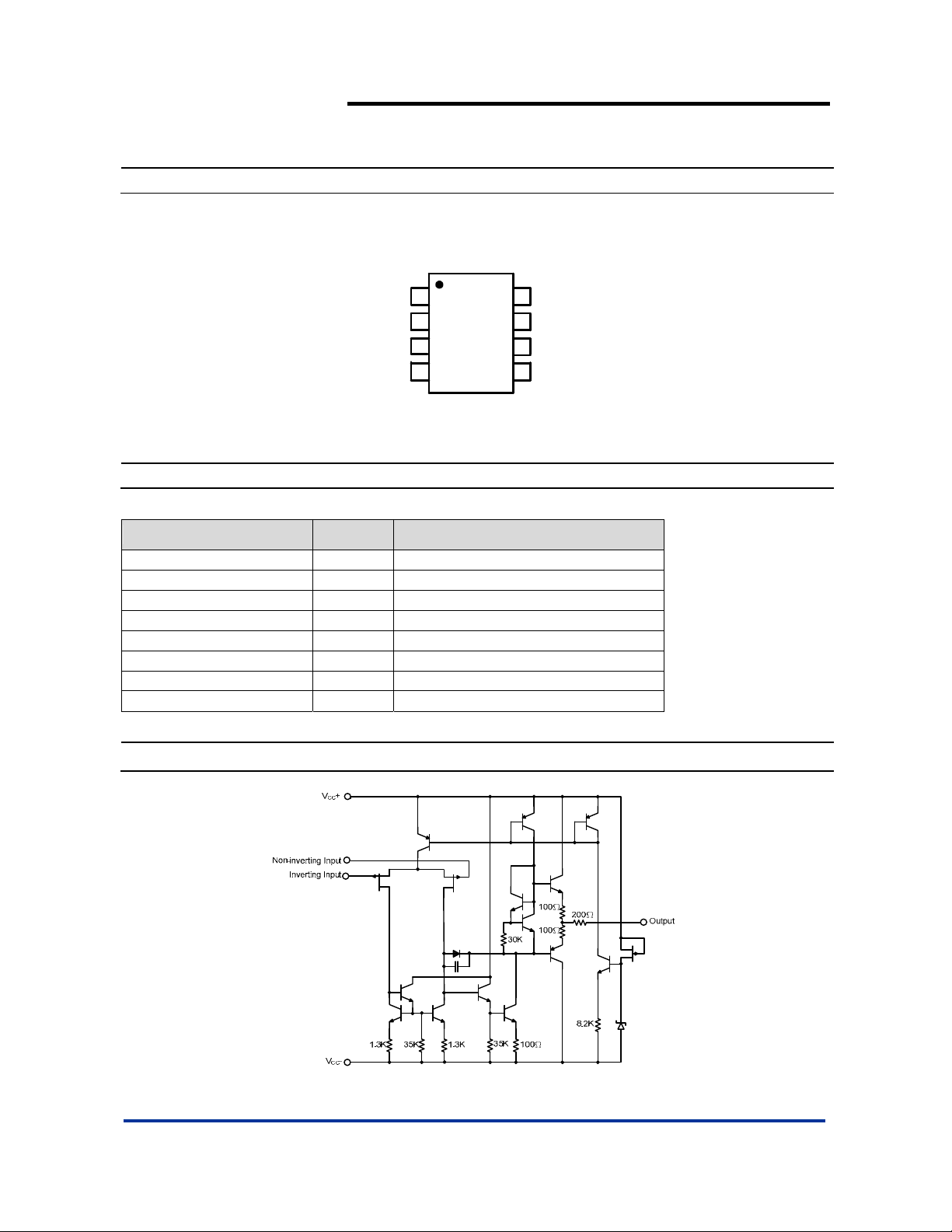
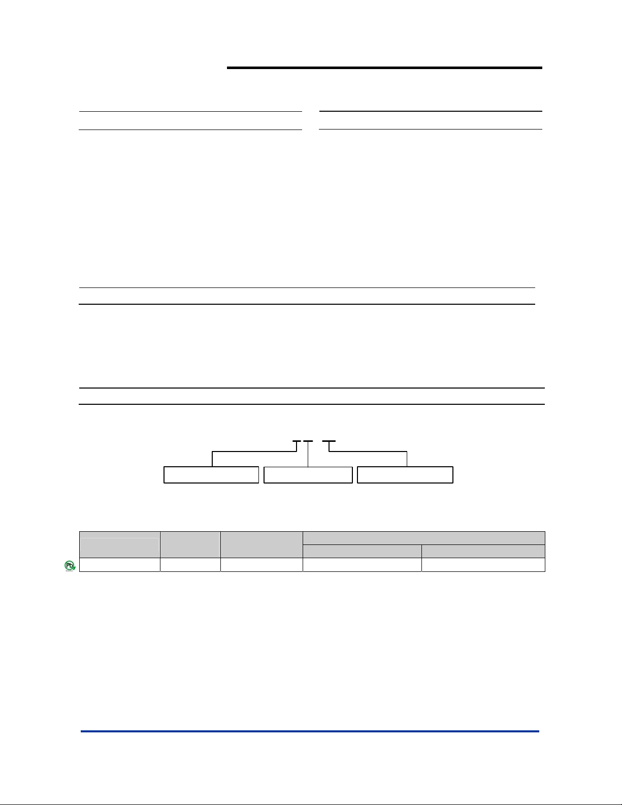
Pin Assignments
(1) Dual channel SOP-8L
TL082
GENERAL PURPOSE JFET INPUT OPERATIONAL
AMPLIFIERS
( Top View )
OUTPUT1
INVERTING INPUT1
NON-INVERTING INPUT1
V
CC
1
2
TL082
3
-
45
V
8
CC+
7
OUTPUT2
INVERTING INPUT2
6
NON-INVERTING INPUT2
SOP-8L
Pin Descriptions
Pin Name Pin No. Description
OUTPUT1 1 Channel 1 Output
INVERTING INPUT1 2 Channel 1 Inverting Input
NON-INVERTING INPUT1 3 Channel 1 Non-inverting Input
VCC- 4 Supply Voltage
NON-INVERTING INPUT2 5 Channel 2 Non-inverting Input
INVERTING INPUT2 6 Channel 2 Inverting Input
OUTPUT2 7 Channel 2 Ouput
VCC+ 8 Supply Voltage
Block Diagram
TL082 Rev. 1 2 of 11 JULY 2009
www.diodes.com © Diodes Incorporated
Page 3
TL082
GENERAL PURPOSE JFET INPUT OPERATIONAL
AMPLIFIERS
Absolute Maximum Ratings (Note 8)
Symbol Parameter Rating Unit
VCC+ Supply Voltage + (Note 3) +18 V
VCC- Supply Voltage - (Note 3) -18 V
VI Input voltage (Notes 3 and 5) ±15 V
VID Differential input Voltage, V
Duration of output short circuit (Note 6) Unlimited
PD Power Dissipation (Note 7) 860 mW
TJ Operating Junction Temperature Range 150
TST Storage Temperature Range -65 to +150
Notes: 3. ALL voltage values, except differential voltages, are with respect to the midpoint between V
4. Differential voltage are at the non-inverting input terminal with respect to the inverting input terminal.
5. The magnitude of the input voltage must never exceed the magnitude of the supply voltage or 15V, whichever is less.
6. The output may be shorted to ground or either supply. Temperature and/or supply voltage must be limited to ensure that the dissipation rating is
not exceeded.
7. Maximum power dissipati on is a function of T
temperature is P
=(TJ(max)-TA)/ θJA . Operating at the absolute maximum TJ of 150℃ can affect reliability
D
Recommended Operating Conditions (Note 8)
Symbol Description Rating Unit
VCC± Supply Voltage
TA Operating Ambient Temp erature Ran ge
Notes: 8. Absolute Maximum Ratings indicate limits beyond which damage to the device may occur. Recommended Operating Conditions indicate
TL082 Rev. 1 3 of 11 JULY 2009
conditions for which the device is intended to be functional, but specific performance is not guaranteed. For guaranteed specifications and the
test conditions, see the Electrical Characteristics.
(Note 4)
ID
+ and V
CC
(max), θJA, and TA. The maximum allowable power dissipation at any allowable ambient
J
-.
CC
±30
±15
-40 to +85
V
o
o
V
°C
C
C
www.diodes.com © Diodes Incorporated
Page 4
TL082
GENERAL PURPOSE JFET INPUT OPERATIONAL
AMPLIFIERS
Electrical Characteristics (V
= ±15V, TA = 25
CC±
Symbol Parameter Test Conditions Min Typ. Max Unit
V
=0,
VIO Input Offset Voltage
α
Temperature Coefficient
vIO
of Input Offset Voltage
O
R
=50Ω
S
VO=0, RS=50Ω, TA= full range 18 μV/ oC
IIO Input Offset Current VO=0
IIB Input Bias Current VO=0
V
VOM
AVD
Common Mode
ICR
Input Voltage Range
Maximum Peak
Output Volt age Swing
Large Signal Differential
Voltage Amplification
±11 -12~+15 V
=10kΩ, TA=25oC ±12 ±13.5
R
L
RL≧10kΩ,
RL≧2kΩ
=±10V,
V
O
R
≧2kΩ
L
B1 Unity Gain Bandwidth 3 MHz
ri Input Resistance TA=25 oC
CMRR
k
SVR
ICC
Common Mode
Rejection Ratio
Supply Voltage
Rejection Ratio
(ΔV
±/ΔVIO)
CC
Supply Current
(each amplifier)
V
IC=VICRmin
R
=50Ω, TA=25 oC
S
V
CC
V
=0
O
=50Ω, TA=25 oC
R
S
V
=0, TA=25oC
O
No load
, VO=0
=±9 to ±15V
VO1/VO2 Crosstalk Attenuation AVD=100, TA=25oC 120 dB
V
=10V, CL=100pF,
I
SR Slew Rate at Unity Gain
R
L
=2kΩ
(See Figure 1)
tr Rise Time
Overshoot Factor 20 %
Equivalent Input Noise
Vn
Voltage
Equivalent Input Noise
In
Current
THD
Notes: 9. Test condition for SOP-8L: Devices mounted on FR-4 substrate PC board, with minimum recommended pad layout.
Total Harmonic
Distortion
Thermal Resistance
θ
JA
Junction-to-Ambient
Thermal Resistance
θ
JC
Junction-to-Case
V
=20mV, RL=2kΩ, CL=100pF
I
(See Figure 1)
R
S
=20Ω
f=1kHz 18
f=10 Hz to 10kHz 4 μV
RS=20Ω, f=1kHz 0.01
=6V, AVD=1,
V
Irms
R
≧2kΩ, RS≦1kΩ,
L
f=1kHz
SOP-8L (Note 9) 145
SOP-8L (Note 9) 35
o
C; unless otherwise noted)
=25oC 3 6
T
A
TA= full range 9
=25oC 5 100 pA
T
A
mV
TA= full range 10 nA
=25oC 30 200 pA
T
A
TA= full range 20 nA
= full range
T
A
=25oC 50 200
T
A
±12
±10 ±12
TA= full range 25
12
10
V
V/mV
Ω
75 86 dB
80 86 dB
1.4 2.8 mA
T
=25 oC 8 13
A
V/μs
TA= full range 5
0.05 μs
ΗΖnV
HZpA
0.003 %
o
C/W
o
C/W
TL082 Rev. 1 4 of 11 JULY 2009
www.diodes.com © Diodes Incorporated
Page 5

V
p
g
(
)
V
V
V
GENERAL PURPOSE JFET INPUT OPERATIONAL
Typical Performance Characteristics
Maximum Peak O utput Volt age vs Supply Voltage
15.0
12.5
10.0
RL=10kΩ
=25
T
℃
A
±V
e
ut Volta
TL082
AMPLIFIERS
Maxim um Peak O ut put Vol t age vs Temper at ur e
15.0
RL=10kΩ
12.5
RL=2kΩ
10.0
7.5
5.0
2.5
-Maximum Peak Out
OM
0
0.0
024681012141618
|Vcc±| Suppl y Vol t age ( V)
7.5
5.0
V
2.5
-Maxi m um Peak O ut put Voltage ( ±V)
OM
0.0
0
=±15V
CC±
See Figure 2
-50 -25 0 25 50 75 100
T
-Free A ir Temper ature (℃)
A
Maximum Peak O ut put Vol t age vs Load Resistance
15.0
V
=±15V
CC±
=25
T
℃
12.5
10.0
-Maxi mum Peak Output Voltage(±V)
OM
A
See Figure 2
7.5
5.0
2.5
0
0.0
100 1000 10000
0.1 0.2 0.4 0.7 1 2 4 7 10
Load Resistance (kΩ)
-Maxi m um Peak O ut put Volt age( ±V)
OM
Maximum Peak Output Voltage vs Frequency
15.0
V
=±15V RL=10kΩ
CC±
=25
T
12.5
10.0
V
=±10V
CC±
7.5
V
5.0
2.5
0
0.0
=±5V
CC±
100 1k 10k 100k 1M 10M
Frequency (Hz)
A
See Figure 2
℃
TL082 Rev. 1 5 of 11 JULY 2009
www.diodes.com © Diodes Incorporated
Page 6

V
V
GENERAL PURPOSE JFET INPUT OPERATIONAL
Typical Performance Characteristics (Continued)
Maximum Peak O ut put Vol t age vs Fr equency
15.0
V
=±15V
12.5
10.0
7.5
CC±
V
=±10V
CC±
RL=2kΩ
=25
T
℃
A
See Figure 2
Maxi m um Peak Output Voltage vs Fr equenc y
15.0
12.5
10.0
TA=-40
7.5
TL082
AMPLIFIERS
V
=±15V
TA=25
CC±
=2kΩ
R
L
See Figu re 2
℃
℃
5.0
V
=±5V
CC±
2.5
-Maxi mum Peak O ut put Voltage(±V)
OM
0
0.0
100 1k 10k 100k 1M 10M
Frequency ( Hz)
5.0
TA=85
2.5
-Maxim um Peak O utput Vol tage( ±V)
OM
0
0.0
10k 40k 100k 400k 1M 4M 10M
℃
Frequency ( Hz)
Input Bi as Curr e nt vs Tem pe r ature
100.00
100
V
=±15V
CC±
10
10.00
1
1.00
0.1
0.10
-Input Bi as Curr ent ( nA)
IB
I
0.01
0.01
-50 -25 0 25 50 75 100
-Free A i r Tem perature (℃)
T
A
Differential Voltage Amplification vs Temperature
1000
1000
400
200
100
100
40
20
10
10
V
=±15V
CC±
40
=±10V
V
O
20
-Differential Voltage Amplification (V/mV)
VD
A
R
=2kΩ
L
1
1
-50 -25 0 25 50 75 100
Large Si gnal
-Free-Air Temperature (℃)
T
A
TL082 Rev. 1 6 of 11 JULY 2009
www.diodes.com © Diodes Incorporated
Page 7

GENERAL PURPOSE JFET INPUT OPERATIONAL
Typical Performance Characteristics (Continued)
TL082
AMPLIFIERS
2.0
1.8
1.6
1.4
1.2
1.0
0.8
0.6
-Supply Current(mA)
0.4
CC±
I
0.2
0.0
0
0246810121416
Supply Current vs Supply Voltage
TA=25
℃
No Signal
No Load
|Vcc±| Supply Volt age (V)
2.4
2.2
2.0
1.8
1.6
1.4
1.2
1.0
0.8
-Supply Curr e nt ( m A)
0.6
CC±
I
0.4
0.2
0.0
0
-50 -25 0 25 50 75 100
Supply Current vs Tem per at ur e
V
=±15V
CC
±
No Signal
No Load
T
-Free Air Temperat ure (℃)
A
Total Power Dissi pat i on vs Tem pera t ure
150
125
100
75
50
V
-Total Power Disspation(mW)
25
D
P
=±15V
CC
±
No Signal
No Load
0
-50 -25 0 25 50 75 100
T
-Free Air Temperature (℃)
A
Mode Reje c tion Ratio(dB)
Common Mode Rej ection Rat io vs Temp er at u re
95
V
=±15V
CC
±
94
=10kΩ
R
L
93
92
91
90
89
88
87
86
85
-50 -25 0 25 50 75 100
-Free Air Te m per at ur e (℃)
T
A
TL082 Rev. 1 7 of 11 JULY 2009
www.diodes.com © Diodes Incorporated
Page 8

V
A
A
A
1
GENERAL PURPOSE JFET INPUT OPERATIONAL
Typical Performance Characteristics (Continued)
TL082
AMPLIFIERS
Equival ent Input Noi se Voltage vs Fr eque ncy
Hz)
50
√
40
30
20
10
0
n - Equiv al e nt Input Noi se Vol tage(nV/
10 40 100 400 1k 4k 10k 40k 100k
10 100 1000 10000 100000
Frequency ( Hz)
V
R
T
CC
VD
=20Ω
S
=25
A
Total Har m onic Distort i o n
vs Frequency
0.4
0.1
0.1
0.04
0.01
0.01
1
1
V
=±15V
CC±
=1
VD
=6V
V
I(RMS)
=25
T
℃
=±15V
±
=10
℃
Output Vol t a ge vs El apse d Ti m e
28
24
20
16
V
=±5V
12
8
-Output Voltage(mV)
O
4
V
0
-4
-0.4 -0.2 0 0.2 0.4 0.6 0.8 1 1.2
Large- Singnal Pulse Respons e
6
4
2
0
-2
Input
CC±
R
=2kΩ
L
=100pF
C
L
=25
T
℃
A
See Figure 1
t-Elapsed Time-μs
Voltage-Follower
V
CC±
R
=2kΩ
L
=100pF
C
L
T
=25
A
Output
=±5V
℃
0.004
Total Har m onic Dist or t ion(% )
0.001
0.001
100 400 1k 4k 10k 40k 100k
0.1 1 10 100
Frequency(Hz)
-4
Input and O utput Vol tages(V)
-6
-0.5 0 0.5 1 1.5 2 2.5 3 3.5
t-Time-μs
TL082 Rev. 1 8 of 11 JULY 2009
www.diodes.com © Diodes Incorporated
Page 9

Test Circuit
V
I
CL=100pF
Figure 1. Unity-Gain Amplifier Figure 2. Gain-of-10 Inverting Amplifier
Marking Information
(1) SOP-8L
GENERAL PURPOSE JFET INPUT OPERATIONAL
OUT
RL=2kΩ
( Top View )
TL082
AMPLIFIERS
10kΩ
1kΩ
V
I
OUT
R
L
CL=100pF
8
Logo
Part Number
TL082
WW X
YY
5
G : Green
YY
: Year : 08, 09,10~
X
41
WW : Week : 01~52; 52
represents 52 and 53 week
X
: Internal Code
TL082 Rev. 1 9 of 11 JULY 2009
www.diodes.com © Diodes Incorporated
Page 10

GENERAL PURPOSE JFET INPUT OPERATIONAL
Package Information ( All Dimensions in mm )
(1) Package type: SOP-8L
0.254
3.85/3.95
5.90/6.10
0.10/0.20
Detail "A"
0.62/0.82
Gauge Plane
Seating Plane
TL082
AMPLIFIERS
7°~9°
1.27typ
8x-0.60
6x-1.27
8x-1.55
Land Pattern Recommendation
0.3/0.5
4.85/4.95
(Unit: mm)
5.4
1.30/1.50
1.75max.
0.35max.
0.15/0.25
7°~9°
45°
Detail "A"
0°/8°
TL082 Rev. 1 10 of 11 JULY 2009
www.diodes.com © Diodes Incorporated
Page 11

TL082
GENERAL PURPOSE JFET INPUT OPERATIONAL
AMPLIFIERS
DIODES INCORPORATED MAKES NO WARRANTY OF ANY KIND, EXPRESS OR IMPLIED, WITH REGARDS TO THIS
DOCUMENT, INCLUDING, BUT NOT LIMITED TO, THE IMPLIED WARRANTIES OF MERCHANTABILITY AND FITNESS FOR A
PARTICULAR PURPOSE (AND THEIR EQUIVALENTS UNDER THE LAWS OF ANY JURISDICTION).
Diodes Incorporated and its subsidiaries reserve the right to make modifications, enhancements, improvements, corrections or other
changes without further notice to this document and any product described herein. Diodes Incorporated does not assume any liability
arising out of the application or use of this document or any product described herein; neither does Diodes Incorporated convey any
license under its patent or trademark rights, nor the rights of others. Any Customer or user of this document or products described
herein in such applications shall assume all risks of such use and will agree to hold Diodes Incorporated and all the companies
whose products are represented on Diodes Incorporated website, harmless against all damages.
Diodes Incorporated does not warrant or accept any liability whatsoever in respect of any products purchased through unauthorized
sales channel.
Should Customers purchase or use Diodes Incorporated products for any unintended or unauthorized application, Customers shall
indemnify and hold Diodes Incorporated and its representatives harmless against all claims, damages, expenses, and attorney fees
arising out of, directly or indirectly, any claim of personal injury or death associated with such unintended or unauthorized application.
Products described herein may be covered by one or more United States, international or foreign patents pending. Product names
and markings noted herein may also be covered by one or more United States, international or foreign trademarks.
Diodes Incorporated products are specifically not authorized for use as critical components in life support devices or systems without
the express written approval of the Chief Executive Officer of Diodes Incorporated. As used herein:
A. Life support devices or systems are devices or systems which:
1. are intended to implant into the body, or
2. support or sustain life and whose failure to perform when properly used in accordance with instructions for use provided
in the labeling can be reasonably expected to result in significant injury to the user.
B. A critical component is any component in a life support device or system whose failure to perform can be reasonably expected
to cause the failure of the life support device or to affect its safety or effectiveness.
Customers represent that they have all necessary expertise in the safety and regulatory ramifications of their life support devices or
systems, and acknowledge and agree that they are solely responsible for all legal, regulatory and safety-related requirements
concerning their products and any use of Diodes Incorporated products in such safety-critical, life support devices or systems,
notwithstanding any devices- or systems-related information or support that may be provided by Diodes Incorporated. Further,
Customers must fully ind emnify Diodes Incorpor ated and its representatives against any damages arising out of the use of Diodes
Incorporated products in such safety-critical, life support devices or systems.
Copyright © 2009, Diodes Incorporated
www.diodes.com
IMPORTANT NOTICE
LIFE SUPPORT
TL082 Rev. 1 11 of 11 JULY 2009
www.diodes.com © Diodes Incorporated
 Loading...