

Page 1
Please click here to visit our online spice models database.
TL072
LOW NOISE JFET INPUT OPERATIONAL
AMPLIFIERS
Features
• Low Power Consumption
• Wide Common-Mode and Differential Voltage Ranges
• Low Input Bias and Offset Currents
• Output Short-Circuit Protection
• Low Total Harmonic Distortion…0.003% Typ
• Low Noise Vn=
• High Input Impedance…JFET-Input Stage
• Internal Frequency Compensation
• Latch-Up-Free Operation
• High Slew Rate…13V/μs Typ
• Common-Mode Input Voltage Range Includes V
• SOP-8L: Available in “Green” Molding Compound
(No Br, Sb)
• Lead Free Finish/ RoHS Compliant (Note 1)
ΗΖ18nV Typ at f=1kHz
Applications
• Active filters
• Audio pre-amps
Ordering Information
TL 072 S G - 13
General Description
The JFET-input operational amplifiers in the TL072 are similar to
the TL082, with low input bias and offset currents and fast slew
rate. The low harmonic distortion and low noise make the TL072
ideally suited for high-fidelity and audio preamplifier applications.
Each amplifier features JFET inputs (for high input impedance)
coupled with bipolar output stages integrated on a single
monolithic chip.
+
CC
Package Packing
S : SOP-8L
Green
G : Green
13 : Tape & Reel
Device
Package
Code
Packaging
(Note 2)
13” Tape and Reel
Quantity Part Number Suffix
TL072SG-13 S SOP-8L 2500/Tape & Reel -13
Notes: 1. EU Directive 2002/95/EC (RoHS). All applicable RoHS exemptions applied. Please visit our website at
http://www.diodes.com/datasheets/ap02001.pdf.
http://www.diodes.com/products/lead_free.html
2. Pad layout as shown on Diodes Inc. suggested pad layout document AP02001, which can be found on our website at
TL072 Rev. 1 1 of 11 MAY 2009
www.diodes.com © Diode s Incorporated
Page 2
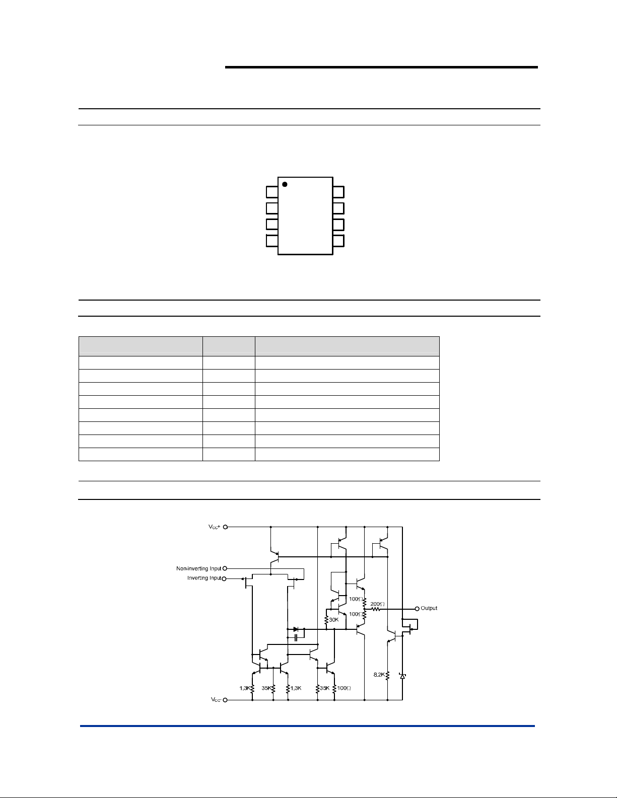
Pin Assignments
(1) Dual channel SOP-8L
TL072
LOW NOISE JFET INPUT OPERATIONAL
AMPLIFIERS
( Top View )
OUTPUT1
INVERTING INPUT1
NON-INVERTING INPUT1
V
CC
1
2
TL072
3
-
45
V
8
CC+
7
OUTPUT2
6
INVERTING INPUT2
NON-INVERTING INPUT2
SOP-8L
Pin Descriptions
Pin Name Pin No. Description
OUTPUT1 1 Channel 1 Output
INVERTING INPUT1 2 Channel 1 Inverting Input
NON-INVERTING INPUT1 3 Channel 1 Non-inverting Input
VCC- 4 Supply Voltage
NON-INVERTING INPUT2 5 Channel 2 Non-inverting Input
INVERTING INPUT2 6 Channel 2 Inverting Input
OUTPUT2 7 Channel 2 Ouput
VCC+ 8 Supply Voltage
Block Diagram
TL072 Rev. 1 2 of 11 JULY 2009
www.diodes.com © Diodes Incorporated
Page 3
TL072
LOW NOISE JFET INPUT OPERATIONAL
AMPLIFIERS
Absolute Maximum Ratings (Note 8)
Symbol Parameter Rating Unit
ESD HBM Human Body Model ESD Protection 1 KV
ESD MM Machine Model ESD Protection 200 V
VCC+ Supply Voltage + (Note 3) +18 V
VCC- Supply Voltage - (Note 3) -18 V
VI Input voltage (Notes 3 and 5) ±15 V
VID Differential input Voltage, V
Duration of output short circuit (Note 6) Unlimited
PD Power Dis sipation (Note 7) 860 mW
TJ Operating Junction Temperature Range 150
TST Storage Temperature Range -65 to +150
Notes: 3. ALL voltage values, except differential voltages, are with respect to the midpoint between V
4. Differential voltage are at the non-inverting input terminal with respect to the inverting input terminal.
5. The magnitude of the input voltage must never exceed the magnitude of the supply voltage or 15V, whichever is less.
6. The output may be shorted to ground or either supply. Temperature and/or supply voltage must be limited to ensure that the dissipation rating is
not exceeded.
7. Maximum power dissipation is a function of T
temperature is P
=(TJ(max)-TA)/ θJA . Operating at the absolute maximum TJ of 150℃ can affect reliability
D
Recommended Operating Conditions (Note 8)
Symbol Description Rating Unit
VCC± Supply Voltage
TA Operating Ambient Temperature Range
Notes: 8. Absolute Maximum Ratings indicate limits beyond which damage to the device may occur. Recommended Operating Conditions indicate
conditions for which the device is intended to be functional, but specific performance is not guaranteed. For guaranteed specifications and the
test conditions, see the Electrical Characteristics.
(Note 4)
ID
+ and V
CC
CC
(max), θJA, and TA. The maximum allowable power dissipation at any allowable ambient
J
±30
-.
±15
-40 to +85
V
o
C
o
C
V
°C
TL072 Rev. 1 3 of 11 JULY 2009
www.diodes.com © Diodes Incorporated
Page 4
TL072
LOW NOISE JFET INPUT OPERATIONAL
AMPLIFIERS
Electrical Characteristics (V
= ±15V, TA = 25
CC±
Symbol Parameter Test Conditions Min Typ. Max Unit
=25oC 3 6
V
VIO Input Offset Voltage
α
vIO
Temperature Coefficient
of Input Offset Voltage
O
R
S
VO=0, RS=50Ω, TA= full range 18 μV/ oC
IIO Input Offset Current VO=0
IIB Input Bias Current VO=0
V
VOM
AVD
Common Mode
ICR
Input Voltage Range
Maximum Peak
Output Voltage Swing
Large Signal Di f ferential
Voltage Amplification
±11 -12~+15 V
R
L
RL≧10kΩ,
RL≧2kΩ
V
O
R
L
=0,
=50Ω
=10kΩ, TA=25oC ±12 ±13.5
=±10V,
≧2kΩ
T
A
TA= full range 8
=25oC 5 100 pA
T
A
TA= full range 2 n A
=25oC 65 200 pA
T
A
TA= full range 20 nA
T
= full range
A
=25oC 50 200
T
A
TA= full range 25
B1 Unity Gain Bandwidth 3 MHz
ri Input Resistance TA=25oC
CMRR
k
SVR
ICC
Common Mode
Rejection Rati o
Supply Voltage
Rejection Rati o
±/ΔVIO)
(ΔV
CC
Supply Current
(each amplifier)
V
IC=VICRmin
=50Ω, TA=25 oC
R
S
V
CC
V
=0
O
=50Ω, TA=25 oC
R
S
V
=0, TA=25oC
O
No load
, VO=0
=±9 to ±15V
VO1/VO2 Crosstalk Attenuation AVD=100, TA=25oC 120 dB
=10V, CL=100pF, RL=2kΩ
V
SR Slew Rate at Unity Gain
tr Rise Time
Overshoot Factor 20 %
Vn
In
THD
θ
θ
Notes: 9. Test condition for SOP-8L: Devices mounted on FR-4 substrate PC board, with minimum recommended pad layout.
Equivalent Input Noise
Voltage
Equivalent Input Noise
Current
Total Harmonic
Distortion
Thermal Resistance
JA
Junction-to-Ambient
Thermal Resistance
JC
Junction-to-Case
I
(See Figure 1)
=20mV, RL=2kΩ, CL=100pF
V
I
(See Figure 1)
RS=20Ω
f=1kHz 18
f=10 Hz to 10kHz 4 μV
RS=20Ω, f=1kHz 0.01
=6V, AVD=1,
V
Irms
R
≧2kΩ, RS≦1kΩ,
L
f=1kHz
SOP-8L (Note 9) 145 oC/W
SOP-8L (Note 9) 35
TL072 Rev. 1 4 of 11 JULY 2009
www.diodes.com © Diodes Incorporated
o
C; unless otherwise noted)
±12
±10
12
10
75 100 dB
80 100 dB
1.4 2.5 mA
8 13 V/μs
0.1 μs
0.003 %
mV
V
V/mV
Ω
o
C/W
HZnV
HZpA
Page 5

V
V
V
V
Typical Performance Characteristics
Maxi mu m Peak Output Volta ge vs Supply Voltage
15.0
RL=10kΩ
=25
T
℃
A
12.5
10.0
TL072
LOW NOISE JFET INPUT OPERATIONAL
AMPLIFIERS
Maximum Peak O ut put Volt age vs Tem perat ur e
15.0
RL=10kΩ
12.5
10.0
RL=2kΩ
7.5
5.0
-Maxi m um Peak O ut put Vol t age( ±V)
2.5
OM
0.0
0
0 2 4 6 8 10 12 14 16 18
|Vcc±| Suppl y Voltage (V)
7.5
5.0
-Maxim um Peak Out put Vol t age( ±V)
2.5
V
=±15V
OM
0.0
CC±
See Figure 2
0
-50 -25 0 25 50 75 100
TA-Free Air Tem perature (℃)
Maxim um Peak O u tput Vol t age vs Load Resi st ance
15.0
V
=±15V
CC±
=25
T
℃
12.5
10.0
-Maximum Peak Out put Voltage(±V)
OM
A
See Figure 2
7.5
5.0
2.5
0.0
0
0.1 0.2 0.4 0.7 1 2 4 7 10
10 100 1000
Load Resistance (kΩ)
-Maxi m um Peak Output Voltage(±V)
OM
Maxim um Peak O utput Voltage vs Frequency
15.0
12.5
10.0
7.5
5.0
2.5
0
0.0
V
=±15V
CC±
V
=±10V
CC±
V
=±5V
CC±
100 1k 10k 100k 1M 10M
Frequency (Hz)
RL=10kΩ
=25
T
℃
A
See Figure 2
TL072 Rev. 1 5 of 11 JULY 2009
www.diodes.com © Diodes Incorporated
Page 6

V
V
LOW NOISE JFET INPUT OPERATIONAL
Typical Performance Characteristics (Continued)
TL072
AMPLIFIERS
Maxim um Peak O utput Voltage vs Frequency
15.0
V
=±15V
CC±
V
=±10V
CC±
V
=±5V
CC±
100 1k 10k 100k 1M 10M
Frequency (Hz)
-Maximum Peak Output Voltage(±V)
OM
12.5
10.0
7.5
5.0
2.5
0
0.0
RL=2kΩ
=25
T
A
See Figure 2
℃
-Maximum Peak Output Voltage(±V)
OM
Maxim um Peak Output Voltage vs Fr equency
15.0
12.5
10.0
7.5
5.0
2.5
0.0
0
10000 100000 1000000 10000000
10k 40k 100k 400k 1M 4M 10M
TA=25
℃
TA=85
TA=-40
℃
℃
Frequen cy (Hz)
V
=±15V
CC±
=2kΩ
R
L
See Figure 2
Input Bias Current vs Temperature
100.00
100
V
=±15V
CC±
10.00
10
1
1.00
0.10
0.1
-Input Bias Curre nt ( nA)
IB
I
0.01
0.01
-50 -25 0 25 50 75 100
T
-Free A ir Temperature (℃)
A
1000.0
-Differential Voltage Amplification (V/mV)
VD
A
Differential Vol t a ge Amplification vs Tempera t ur e
1000
400
200
100
100.0
40
20
10
10.0
V
=±15V
CC±
=±10V
V
O
=2kΩ
R
L
-50 -25 0 25 50 75 100
T
1.0
4
2
1
Large Signal
-Free-Ai r Temperatur e ( ℃)
A
TL072 Rev. 1 6 of 11 JULY 2009
www.diodes.com © Diodes Incorporated
Page 7

pp
y
(
)
p
(
)
LOW NOISE JFET INPUT OPERATIONAL
Typical Performance Characteristics (Continued)
TL072
AMPLIFIERS
Supply Current vs Supply Voltage
2.0
1.8
1.6
mA
1.4
1.2
1.0
Current
l
0.8
0.6
-Su
CC±
I
TA=25
0.4
0.2
0
0.0
℃
No Signal
No Load
0246810121416
|Vcc±| Suppl y Voltage (V)
2.4
2.2
2.0
1.8
1.6
1.4
1.2
1.0
0.8
-Supply Curr ent(mA)
0.6
CC±
I
0.4
0.2
0
0.0
-50 -25 0 25 50 75 100
Supply Current v s Tem perature
V
=±15V
CC
±
No Signal
No Load
-Free A i r Temperature (℃)
T
A
Total Power Di ssi pation vs Temperatur e
150
125
mW
ation
100
75
50
V
=±15V
CC
-Total Power Diss
D
P
±
25
No Signal
No Load
0
-50 -25 0 25 50 75 100
T
-Free A ir Temperature (℃)
A
Common Mode Rej ect ion Ratio vs Temperat ur e
98
V
=±15V
CC
±
97
R
=10kΩ
L
96
95
94
93
92
91
90
CMRR -Common- M ode Rej ec t ion Ratio(dB)
-50 -25 0 25 50 75 100
-Free A ir Temperature (℃)
T
A
TL072 Rev. 1 7 of 11 JULY 2009
www.diodes.com © Diodes Incorporated
Page 8

A
V
A
LOW NOISE JFET INPUT OPERATIONAL
Typical Performance Characteristics (Continued)
Equivale nt Input Noise Volt age v s Fr equenc y
50
Hz)
√
40
30
20
V
R
T
CC±
VD
=20Ω
S
=25
A
=±15V
=10
℃
6
4
2
0
-2
AMPLIFIERS
Voltage-Follower
Large-Singnal Pulse Response
Input
TL072
V
=±5V
CC±
R
=2kΩ
L
C
=100pF
L
=25
T
℃
A
Output
10
n - Equiva lent Input Nois e Voltage(nV/
0
10 100 1000 10000 100000
10 40 100 400 1k 4k 10k 40k 100k
Frequency (Hz)
-4
Input and Output Volta ges(V)
-6
-0.5 0 0.5 1 1.5 2 2.5 3 3.5
t-Time-μs
Total Har m oni c Di st ortion vs Frequency
1
1
V
=±15V
CC±
Total Har m oni c Di st or t i on( % )
0.001
0.4
0.1
0.1
0.04
0.01
0.01
0.00
0.001
=1
VD
V
=6V
I(RMS)
T
=25
℃
A
100 400 1k 4k 10k 40k 100k
0.1 1 10 100
Frequency(Hz)
28
24
20
16
12
8
-Out put Vol t age( m V)
O
4
V
0
-4
-0.1 0 0.1 0.2 0.3 0.4 0.5 0.6 0.7
10%
Output Vol tage vs Elapsed Time
Overshoot
90
V
R
T
tr
t-El aps ed Ti m e- μs
CC±
=2kΩ
L
=25
A
=±5V
℃
TL072 Rev. 1 8 of 11 JULY 2009
www.diodes.com © Diodes Incorporated
Page 9

r
Test Circuit
V
CL=100pF
Figure 1. Unity-Gain Amplifier Figure 2. Gain-of-10 Inverting Amplifie
Marking Information
(1) SOP-8L
OUT
RL=2kΩ
( Top View )
TL072
LOW NOISE JFET INPUT OPERATIONAL
AMPLIFIERS
10kΩ
1kΩ
V
OUT
R
L
CL=100pF
8
Logo
Part Number
TL072
WW X
YY
5
G : Green
YY
: Year : 08, 09,10~
X
41
WW : Week : 01~52; 52
represents 52 and 53 week
X
: Internal Code
TL072 Rev. 1 9 of 11 JULY 2009
www.diodes.com © Diodes Incorporated
Page 10

LOW NOISE JFET INPUT OPERATIONAL
Package Information ( All Dimensions in mm )
(1) Package type: SOP-8L
0.254
3.85/3.95
5.90/6.10
0.10/0.20
Detail "A"
0.62/0.82
Gauge Plane
Seating Plane
TL072
AMPLIFIERS
7°~9°
1.27typ
8x-0.60
6x-1.27
8x-1.55
Land Pattern Recommendation
0.3/0.5
4.85/4.95
(Unit: mm)
5.4
1.30/1.50
1.75max.
0.35max.
0.15/0.25
7°~9°
45°
Detail "A"
0°/8°
TL072 Rev. 1 10 of 11 JULY 2009
www.diodes.com © Diodes Incorporated
Page 11

TL072
LOW NOISE JFET INPUT OPERATIONAL
AMPLIFIERS
DIODES INCORPORATED MAKES NO WARRANTY OF ANY KIND, EXPRESS OR IMPLIED, WITH REGARDS TO THIS
DOCUMENT, INCLUDING, BUT NOT LIMITED TO, THE IMPLIED WARRANTIES OF MERCHANTABILITY AND FITNESS FOR A
PARTICULAR PURPOSE (AND THEIR EQUIVALENTS UNDER THE LAWS OF ANY JURISDICTION).
Diodes Incorporated and its subs idiaries reserve the right to make modific ations, enhancem ents, improvem ents, correctio ns or other
changes without further notic e to this document and any product des cri bed herein. Diodes Inc orporat ed does not assum e any liabi lity
arising out of the applicati on or use of this document or any produc t described herein ; neither does Diodes In corporat ed convey any
license under its patent or trademark rights, nor the rights of others . Any Customer or user of t his document or produc ts described
herein in such applications shall assume all risks of such use and will agree to hold Diodes Incorporated and all the companies
whose products are represented on Diodes Incorporated website, harmless against all damages.
Diodes Incorporated do es not warrant or accept an y liabilit y whatsoever in re spect of any product s purchased through unaut horized
sales channel.
Should Customers purchase or use Diod es Incorporated products for any unintend ed or unauthorized application, Custom ers shall
indemnify and hold Diodes Incorpor ated and its repres entatives harmless agai nst all claims, damages , expenses, and atto rney fees
arising out of, directly or indi re ct l y, any c l a im of person al i nj u ry or death ass oci a t e d with suc h uni nte nde d or un authorized application.
Products described h erein may be covered by one or more United States, i nternational or f oreign patents pendi ng. Product names
and markings noted herein may also be covered by one or more Uni ted S tates, international or foreig n tradem a rks.
Diodes Incorporated products are specific ally not authorized for use as critical components in life support devic es or systems without
the express written approval of t he Chief Execut ive Officer of Diodes Incorporated . As used herei n :
A. Life support devices or systems are devices or systems which:
1. are intended to impl ant i nto the body, or
2. support or sustain life and whose failure to perform when properly used in accordanc e with ins t ruc t i ons for use provided
in the labeling can be reasonably expected to result in significant injury to th e user.
B. A critical component is any component in a life support device or system whose failure t o perform can be rea sonably expect ed
to cause the failure of the life support device or to affect its safety or effectiveness.
Customers represent that they have all nec essary expertise in the safet y and regulatory ramificati ons of their life support devices or
systems, and acknowledge and agree that they are solely responsible for all legal, regulatory and safety-related requirements
concerning their products and any use of Diodes Incorporated products in such safety-critical, life support devices or systems,
notwithstanding any devices- or systems-related information or support that may be provided by Diodes Incorporated. Further,
Customers must fully indemnif y Diodes Incorporated and its representati ves against any damages arising out of the use of Diodes
Incorporated products in such safety-critical, life support devices or systems.
Copyright © 2009, Diodes Incorporated
www.diodes.com
IMPORTANT NOTICE
LIFE SUPPORT
TL072 Rev. 1 11 of 11 JULY 2009
www.diodes.com © Diodes Incorporated
 Loading...