

Page 1
100A BIDIRECTIONAL SURFACE MOUNT THYRISTOR SURGE PROTECTIVE DEVICE
Features
• 100A Peak Pulse Current @ 10/1000μs
• 400A Peak Pulse Current @ 8/20μs
• 58 - 320V Stand-Off Voltages
• Oxide-Glass Passivated Junction
• Bidirectional Protection In a Single Device
• High Off-State Impedance and Low On-State Voltage
• Helps Equipment Meet GR-1089-CORE, IEC 61000-4-5, FCC
Part 68, ITU-T K.20/K.21, and UL497B
• UL Listed Under Recognized Component Index, File Number
156346
• Lead Free Finish/RoHS Compliant (Note 1)
• Green Molding Compound (No Halogen and Antimony)
(Note 2)
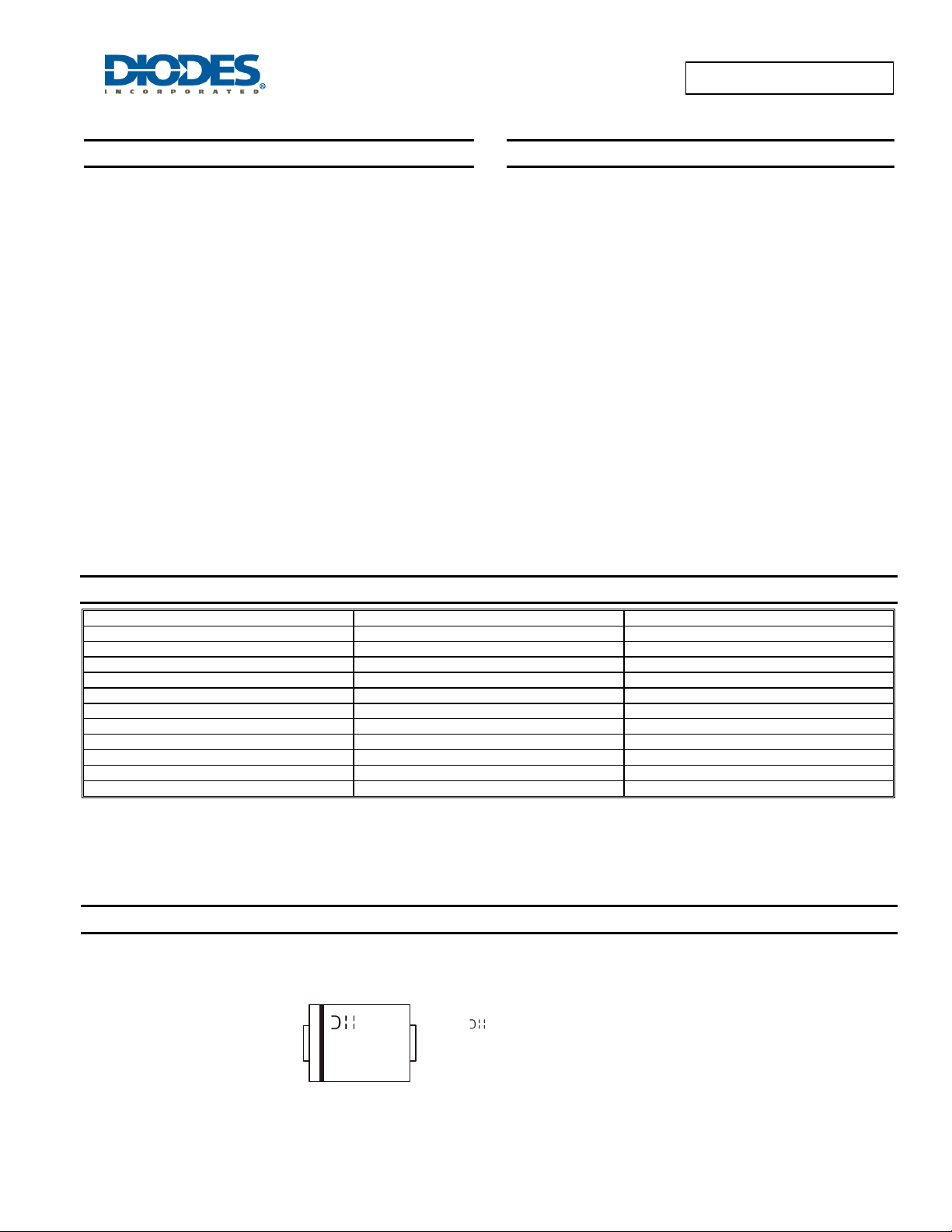
Top View
Green
TB0640H - TB3500H
Mechanical Data
• Case: SMB
• Case Material: Molded Plastic. UL Flammability Classification
Rating 94V-0
• Moisture Sensitivity: Level 1 per J-STD-020
• Terminals: Lead Free Plating (Matte Tin Finish). Solderable per
MIL-STD-202, Method 208
• Polarity: None; Bidirectional Devices Have No Polarity Indicator
• Weight: 0.093 grams (approximate)
Bottom View
Ordering Information (Note 3)
Part Number Case Packaging
TB0640H-13-F SMB 3000/Tape & Reel
TB0720H-13-F SMB 3000/Tape & Reel
TB0900H-13-F SMB 3000/Tape & Reel
TB1100H-13-F SMB 3000/Tape & Reel
TB1300H-13-F SMB 3000/Tape & Reel
TB1500H-13-F SMB 3000/Tape & Reel
TB1800H-13-F SMB 3000/Tape & Reel
TB2300H-13-F SMB 3000/Tape & Reel
TB2600H-13-F SMB 3000/Tape & Reel
TB3100H-13-F SMB 3000/Tape & Reel
TB3500H-13-F SMB 3000/Tape & Reel
Notes: 1. EU Directive 2002/95/EC (RoHS). All applicable RoHS exemptions applied, see EU Directive 2002/95/EC Annex Notes.
2. Product manufactured with Data Code 0924 (week 24, 2009) and newer are built with Green Molding Compound.
3. For packaging details, go to our website at http://www.diodes.com.
Marking Information
TB0640H - TB3500H
Document number: DS30360 Rev. 10 - 2
xxxxx
YWW
xxxxx = Product type marking code (See table on page 2)
= Manufacturers’ code marking
YWW = Date code marking
Y = Last digit of year (ex: 6 for 2006)
WW = Week code (01 to 53)
1 of 6
www.diodes.com
May 2011
© Diodes Incorporated
Page 2
pp
θ
θ
Maximum Ratings @T
= 25°C unless otherwise specified
A
Single phase, half wave, 60Hz, resistive or inductive load.
For capacitance load, derate current by 20%.
Characteristic Symbol Value Unit
Non-Repetitive Peak Impulse Current @10/1000us
Non-Repetitive Peak On-State Current @8.3ms (one-half cycle)
Typical Positive Temperature Coefficient for Breakdown Voltage
Thermal Characteristics
Characteristic Symbol Value Unit
Thermal Resistance, Junction to Lead
Thermal Resistance, Junction to Ambient
Junction Temperature Range
Storage Temperature Range
I
I
TSM
ΔVBR/ΔT
R
JL
R
JA
T
J
T
STG
TB0640H - TB3500H
100 A
J
50 A
0.1 %/°C
20 °C/W
100 °C/W
-40 to +150
-55 to +150
°C
°C
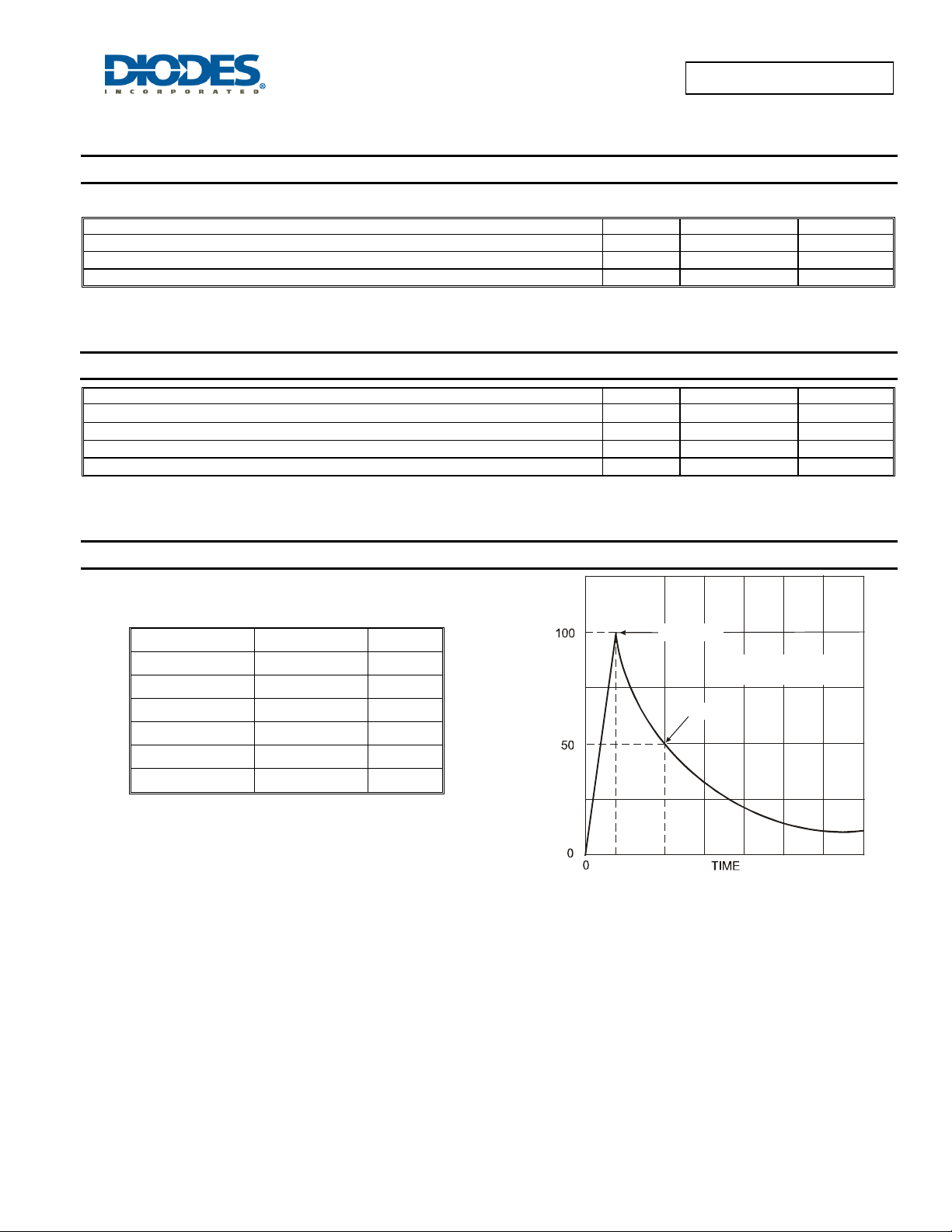
Maximum Rated Surge Waveform
Waveform Standard Ipp (A)
2/10μs
8/20μs
10/160μs
10/700μs (Note 4)
10/560μs
10/1000μs
Notes: 4. Applied 6kV, 10/700μs waveform
GR-1089-CORE 500
IEC 61000-4-5 400
FCC Part 68 250
ITU-T, K.20/K.21 200
FCC Part 68 160
GR-1089-CORE 100
Peak Value (I )
PP
I , PEAK PULSE CURRENT (%)
t
t
r
Half Value
p
pp
t = rise time to peak value
r
t = decay time to half value
p
TB0640H - TB3500H
Document number: DS30360 Rev. 10 - 2
2 of 6
www.diodes.com
May 2011
© Diodes Incorporated
Page 3

TB0640H - TB3500H
Electrical Characteristics @T
Maximum
Off-State
Leakage
Current @
DRM
Part Number
Maximum
Rated
Repetitive
Off-State
Voltage
V
(V) I
DRM
= 25°C unless otherwise specified
A
Maximum
On-State
Voltage
@ I
V
DRM
Maximum
Breakover
Voltage
(uA) VBO (V) VT (V)
= 1A
T
Breakover
Current
I
BO
Min
(mA)
Max
(mA)
Holding Current
I
H
Min
(mA)
Max
(mA)
Typical
Off-State
Capacitance
CO (pF)
Marking
Code
TB0640H 58 5 77 3.5 50 800 150 800 200 T064H
TB0720H 65 5 88 3.5 50 800 150 800 200 T072H
TB0900H 75 5 98 3.5 50 800 150 800 200 T090H
TB1100H 90 5 130 3.5 50 800 150 800 120 T110H
TB1300H 120 5 160 3.5 50 800 150 800 120 T130H
TB1500H 140 5 180 3.5 50 800 150 800 120 T150H
TB1800H 160 5 220 3.5 50 800 150 800 120 T180H
TB2300H 190 5 265 3.5 50 800 150 800 80 T230H
TB2600H 220 5 300 3.5 50 800 150 800 80 T260H
TB3100H 275 5 350 3.5 50 800 150 800 80 T310H
TB3500H 320 5 400 3.5 50 800 150 800 80 T350H
Symbol Parameter
V
DRM
I
DRM
VBR
IBR
VBO
IBO
IH
VT
IPP
CO
Notes: 5. IH > (VL/RL) If this criterion is not obeyed, the TSPD triggers but does not return correctly to high-resistance state. The surge recovery time does not
exceed 30ms.
6. Off-state capa citance measured at f = 1.0MHz, 1.0V
signal, VR = 2VDC bias.
RMS
Stand-off Voltage
Leakage current at stand-off voltage
Breakdown voltage
Breakdown current
Breakover voltage
Breakover current
Holding current (Note 5)
On state voltage
Peak pulse current
Off-state capacitance (Note 6)
I
TB0640H - TB3500H
Document number: DS30360 Rev. 10 - 2
I
PP
I
BO
I
H
I
BR
I
DRM
V
T
3 of 6
www.diodes.com
BR
V
V
BO
May 2011
© Diodes Incorporated
V
V
DRM
Page 4

NOR
R
OWN VOLTAG
O
R
R
O
OLTAG
O
TATE CUR
RENT
O
R
H
O
G C
URRENT
NOR
CAPACIT
N
C
TB0640H - TB3500H
100
1.2
E
10
1.15
1.1
1
1.05
EAKD
0.1
V = 50V
DRM
1
0.01
(DRM)
I , OFF-STATE CURRENT (uA)
0.001
0
-25
25 50 75 100 125 150
T , JUNCTION TEMPERATURE (°C)
J
Fig. 1 Off- Stat e C ur r ent vs. Ju nct ion Tem perature
1.1
MALIZED B
0.95
0.9
-50
-25 0 25
T , JUNCTION TEMPERATURE (°C)
J
50
75 100
Fig. 2 Rela ti ve V ar i at ion of Breakdown Voltag e
vs. Junction Temperature
100
125
150 175
E
WN V
EAKD
1.05
(A)
10
1
MALIZED B
N-S
T
I,
N
0.95
-25
-50
T , JUNCTION TEMPERATURE
25
0
J
50
75
Fig. 3 Rela ti ve V ar i ation of Breakover Voltage
100
125
(ºC)
150
175
1
1
1.5 32.52
V , ON-STATE VOLTAGE (V)
T
3.5
Fig. 4 On-State Current vs. On-State Voltage
5
4.5
4
vs. Junction Tempera tu r e
1.4
1
1.3
1.2
1.1
E
A
1
0.9
LDIN
0.8
0.7
0.6
MALIZED
0.5
N
MALIZED
0.4
0.3
-50 -25
T , JUNCTION TEMPERA TURE (°C)
J
25 50 10075 125
0
Fig. 5 Relative Variation of Holding Current vs.
Junction Temperature
0.1
110100
V , REVERSE VOLTAGE (V)
R
Fig. 6 Relative V ariation of Junction Capacitance
vs. Reverse Vo ltage Bias
TB0640H - TB3500H
Document number: DS30360 Rev. 10 - 2
4 of 6
www.diodes.com
May 2011
© Diodes Incorporated
Page 5

Package Outline Dimensions
A
J
H
TB0640H - TB3500H
B
SMB
C
D
G
E
Dim Min Max
A 3.30 3.94
B 4.06 4.57
C 1.96 2.21
D 0.15 0.31
E 5.00 5.59
G 0.05 0.20
H 0.76 1.52
J 2.00 2.50
All Dimensions in mm
Suggested Pad Layout
X
C
Dimensions Value (in mm)
Z 6.8
G 1.8
X 2.3
Y 2.5
Y
G
Z
C 4.3
TB0640H - TB3500H
Document number: DS30360 Rev. 10 - 2
5 of 6
www.diodes.com
May 2011
© Diodes Incorporated
Page 6

IMPORTANT NOTICE
DIODES INCORPORATED MAKES NO WARRANTY OF ANY KIND, EXPRESS OR IMPLIED, WITH REGARDS TO THIS DOCUMENT,
INCLUDING, BUT NOT LIMITED TO, THE IMPLIED WARRANTIES OF MERCHANTABILITY AND FITNESS FOR A PARTICULAR PURPOSE
(AND THEIR EQUIVALENTS UNDER THE LAWS OF ANY JURISDICTION).
Diodes Incorporated and its subsidiaries reserve the right to make modifications, enhancements, improvements, corrections or other changes
without further notice to this document and any product described herein. Diodes Incorporated does not assume any liability arising out of the
application or use of this document or any product described herein; neither does Diodes Incorporated convey any license under its patent or
trademark rights, nor the rights of others. Any Customer or user of this document or products described herein in such applications shall assume
all risks of such use and will agree to hold Diodes Incorporated and all the companies whose products are represented on Diodes Incorporated
website, harmless against all damages.
Diodes Incorporated does not warrant or accept any liability whatsoever in respect of any products purchased through unauthorized sales channel.
Should Customers purchase or use Diodes Incorporated products for any unintended or unauthorize d application, Customers shall indemnify and
hold Diodes Incorporated and its representatives harmless against all claims, damages, expenses, and attorney fees arising out of, directly or
indirectly, any claim of personal injury or death associated with such unintended or unauthorized application.
Products described herein may be covered by one or more United States, international or foreign patents pending. Product names and markings
noted herein may also be covered by one or more United States, international or foreign trademarks.
LIFE SUPPORT
Diodes Incorporated products are specifically not authorized for use as critical components in life support devices or systems without the express
written approval of the Chief Executive Officer of Diodes Incorporated. As used herein:
A. Life support devices or systems are devices or systems which:
1. are intended to implant into the body, or
2. support or sustain life and whose failure to perform when properly used in accordance with instructions for use provided in the
labeling can be reasonably expected to result in significant injury to the user.
B. A critical component is any component in a life support device or system whose failure to perform can be reasonably expected to cause the
failure of the life support device or to affect its safety or effectiveness.
Customers represent that they have all necessary expertise in the safety and regulatory ramifications of their life support devices or systems, and
acknowledge and agree that they are solely responsible for all legal, regulatory and safety-related requirements concerning their products and any
use of Diodes Incorporated products in such safety-critical, life support devices or systems, notwithstanding any devices- or systems-related
information or support that may be provided by Diodes Incorporated. Further, Customers must fully indemnify Diodes Incorporated and its
representatives against any damages arising out of the use of Diodes Incorporated products in such safety-critical, life support devices or systems.
Copyright © 2011, Diodes Incorporated
www.diodes.com
TB0640H - TB3500H
TB0640H - TB3500H
Document number: DS30360 Rev. 10 - 2
6 of 6
www.diodes.com
May 2011
© Diodes Incorporated
 Loading...