Diodes T12S5 User Manual

Features
Ideally Suited for ESD Protection
Small Surface Mount Package
Excellent Clamping Capability, Fast Response Time
Totally Lead-Free & Fully RoHS Compliant (Notes 1 & 2)
Halogen and Antimony Free. “Green” Device (Note 3)
T3V3S5 / T5V0S5 / T6V0S5 / T12S5
UNIDIRECTIONAL SURFACE MOUNT TVS
Mechanical Data
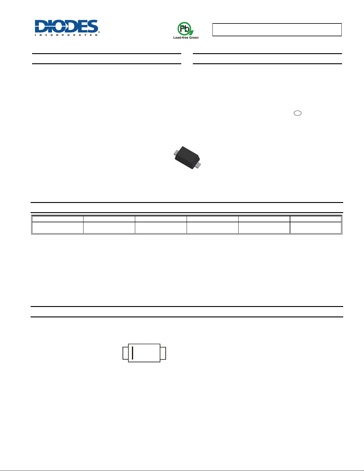
Case: SOD523
Case Material: Molded Plastic, "Green" Molding Compound.
UL Flammability Classification Rating 94V-0
Moisture Sensitivity: Level 1 per J-STD-020
Terminal Connections: Cathode Band
Terminals: Finish - Matte Tin annealed over Alloy 42 leadframe.
Solderable per MIL-STD-202, Method 208
Weight: 0.001 grams (approximate)
Top View
e3
Ordering Information (Note 4)
Product Compliance Marking Reel Size (inches) Tape Width (mm) Quantity per Reel
(Type Number)-7*
(Note 5)
* Add “-7” to the appropriate type number in Electrical Characteristics Table on page 2 example: 5.0V TVS = T5V0S5-7.
Notes: 1. No purposely added lead. Fully EU Directive 2002/95/EC (RoHS) & 2011/65/EU (RoHS 2) compliant.
2. See http://www.diodes.com/quality/lead_free.html for more information about Diodes Incorporated’s definitions of Halogen- and Antimony-free, "Green"
and Lead-free.
3. Halogen- and Antimony-free "Green” products are defined as those which contain <900ppm bromine, <900ppm chlorine (<1500ppm total Br + Cl) and
<1000ppm antimony compounds.
4. For packaging details, go to our website at http://www.diodes.com/products/packages.html
5. Dispensed in every other cavity of the tape.
6. See Electrical Characteristics Table for marking code by part number.
Standard XX (Note 6) 7 8 3,000/Tape & Reel
Marking Information
xx
xx = Product Type Marking Code
(See Electrical Characteristics Table)
T3V3S5 / T5V0S5 / T6V0S5 / T12S5
Document number: DS31112 Rev. 10 - 2
1 of 4
www.diodes.com
August 2013
© Diodes Incorporated

P
P
O
R
PAT
O
T3V3S5 / T5V0S5 / T6V0S5 / T12S5
Maximum Ratings (@T
= +25°C, unless otherwise specified.)
A
Characteristic Symbol Value Unit
Forward Voltage @ IF = 10mA VF
Human Body Model
ESD Rating
Machine Model 400 V
IEC61000-4-2 Air Discharge 30 kV
ESD
0.9 V
8 kV
IEC61000-4-2 Contact Discharge 30 kV
Thermal Characteristics
Characteristic Symbol Value Unit
Power Dissipation (Note 7) (See figure 2)
Thermal Resistance, Junction to Ambient Air (Note 7)
Operating and Storage Temperature Range
P
R
T
J, TSTG
θJA
D
Electrical Characteristics (@T
Part
Number
Reverse
Standoff
Voltage
V
RWM
Breakdown
V
(V)
Min.
Voltage
@ IT
BR
Min (V)
Test
Current
IT (mA) IR (A) V
= +25°C, unless otherwise specified.)
A
Max. Reverse
Leakage @
V
RWM
(Note 8)
Typ. Clamping
Voltage
=5A
@ I
PP
= 8 x 20 s)
(t
p
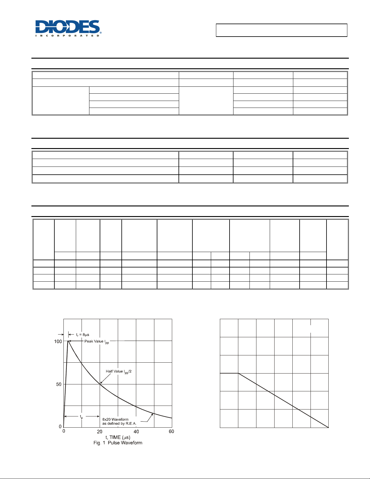
(See figure 1)
(V) V
C
Max. Clamping
(t
(See Figure 1)
Voltage V
@ I
PP1
= 8 x 20 s)
p
(V) I
C
PP
Max. Clamping
Voltage V
c1
= 8 x 20 s)
(t
p
(See Figure 1)
(A) VC (V) I
T3V3S5 3.3 5.0 1.0 1 8.4 14.1 11.2 16 16 220 85 ED
T5V0S5 5.0 6.2 1.0 0.05 15 22 9.4 27 15 260 100 EJ
T6V0S5 6.0 6.8 1.0 0.05 11.6 17 8.8 22.4 13 260 90 EL
T12S5 12 14.1 1.0 0.01 19.7 25 9.6 28 12 300 60 ES
Notes: 7. Part mounted on FR-4 board with recommended pad layout, which can be found on our website at http://www.diodes.com.
8. Short duration pulse test used to minimize self-heating effect.
0.3
150 mW
833 °C/W
-65 to +150 °C
c2
@ I
PP2
(A) PPK (W) C
PP
Peak Power
Dissipation
(See Figure 1)
Typical Total
Capacitance
= 0V
V
R
f = 1MHz
(pF)
T
Note 7
Note 5
Marking
Code
N (W)
I
0.2
DISSI
WE
0.1
,
D
PP pp
I , PEAK PULSE CURRENT (%I )
0
25
050
T , AMBIENT TEMPERATURE ( C)
A
Fig. 2 Power Derating Curve
75
100
125 150
°
T3V3S5 / T5V0S5 / T6V0S5 / T12S5
Document number: DS31112 Rev. 10 - 2
2 of 4
www.diodes.com
August 2013
© Diodes Incorporated
 Loading...