

Page 1
1500W SURFACE MOUNT TRANSIENT VOLTAGE SUPPRESSOR
Features
• 1500W Peak Pulse Power Dissipation
• 5.0V - 170V Standoff Voltages
• Glass Passivated Die Construction
• Unidirectional and Bidirectional Versions Available
• Excellent Clamping Capability
• Fast Response Time
• Lead-Free Finish; RoHS Compliant (Notes 1 & 2)
• Halogen and Antimony Free. “Green” Device (Notes 3 & 4)
• Qualified to AEC-Q101 Standards for High Reliability
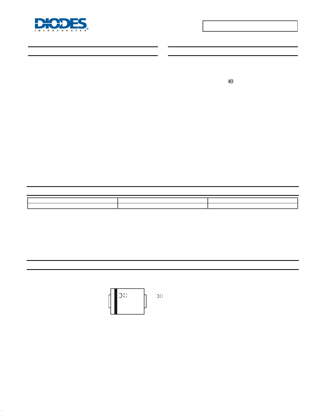
Top View
Green
SMCJ5.0(C)A - SMCJ170(C)A
Mechanical Data
• Case: SMC
• Case Material: Molded Plastic. UL Flammability Classification
Rating 94V-0
• Terminals: Lead Free Plating (Matte Tin Finish). Solderable per
MIL-STD-202, Method 208
• Polarity Indicator: Cathode Band (Note: Bidirectional devices
have no polarity indicator.)
• Weight: 0.21 grams (approximate)
SMC
Bottom View
Ordering Information (Note 5)
Part Number Case Packaging
SMCJXXX(C)A-13-F SMC 3000/Tape & Reel
*x = Device Voltage, e.g., SMCJ170A-13-F.
Notes: 1. EU Directive 2002/95/EC (RoHS) & 2011/65/EU (RoHS 2) compliant. All applicable RoHS exemptions applied.
2. See http://www.diodes.com for more information about Diodes Incorporated’s definitions of Halogen- and Antimony-free, "Green" and Lead-free.
3. Halogen- and Antimony-free "Green” products are defined as those which contain <900ppm bromine, <900ppm chlorine (<1500ppm total Br + Cl) and
<1000ppm antimony compounds.
4. Product manufactured with Date Code 0924 (week 24, 2009) and newer are built with Green Molding Compound.
5. For packaging details, go to our website at http://www.diodes.com.
Marking Information
YWW
xxx
xxx = Product type marking code (See Page 2)
= Manufacturers’ code marking
YWW = Date code marking
Y = Last digit of year (ex: 2 for 2002)
WW = Week code (01 to 53)
SMCJ5.0(C)A - SMCJ170(C)A
Document number: DS19003 Rev. 18 - 2
1 of 6
www.diodes.com
June 2012
© Diodes Incorporated
Page 2
(AV)
Maximum Ratings @T
= 25°C unless otherwise specified
A
Characteristic Symbol Value Unit
Peak Pulse Power Dissipation
(Non repetitive current pulse derated above T
= 25° C) (Note 6)
A
P
Peak Forward Surge Current,
8.3ms Single Half Sine Wave Superimposed on Rated Load
I
(Notes 6, 7, & 8)
Steady State Power Dissipation @ TL = 75°C PM
Instantaneous Forward Voltage @ IPP = 100A (Notes 6 & 8) VF
Thermal Characteristics
Characteristic Symbol Value Unit
Operating Temperature Range
Storage Temperature Range
Notes: 6. Valid provided that terminals are kept at ambient temperature.
9. V
7. Measured with 8.3ms single half sine-wave. Duty cycle = 4 pulses per minute maximum.
8. Unidirectional units only.
= 3.5V for SMCJ5.0A through SMCJ90A, and VF = 5.0V for SMCJ100A through SMCJ170A.
F
T
PK
FSM
T
STG
SMCJ5.0(C)A - SMCJ170(C)A
J
1500 W
200 A
5.0 W
See Note 9 V
-55 to +150
-55 to +175
°C
°C
SMCJ5.0(C)A - SMCJ170(C)A
Document number: DS19003 Rev. 18 - 2
2 of 6
www.diodes.com
June 2012
© Diodes Incorporated
Page 3

SMCJ5.0(C)A - SMCJ170(C)A
Electrical Characteristics @T
Part Number
Add C For
Bidirectional
(Note 10)
Reverse
Standoff
Voltage
V
(V)
RWM
VBR @ IT (Note 11)
Min (V) Max (V)
= 25°C unless otherwise specified
A
Breakdown
Voltage
Test
Current
IT(mA) IR (μA) VC (V)
Max. Reverse
Leakage @
V
(Note 12)
RWM
Max. Clamping
Voltage @ Ipp
Max. Peak Pulse
Current Ipp
(A) BI UNI
Marking Code
SMCJ5.0(C)A 5.0 6.40 7.07 10 1000 9.2 163.0 BDE GDE
SMCJ6.0(C)A 6.0 6.67 7.37 10 1000 10.3 145.6 BDG GDG
SMCJ6.5(C)A 6.5 7.22 7.98 10 500 11.2 133.9 BDK GDK
SMCJ7.0(C)A 7.0 7.78 8.60 10 200 12.0 125.0 BDM GDM
SMCJ7.5(C)A 7.5 8.33 9.21 1.0 100 12.9 116.3 BDP GDP
SMCJ8.0(C)A 8.0 8.89 9.83 1.0 50 13.6 110.3 BDR GDR
SMCJ8.5(C)A 8.5 9.44 10.4 1.0 20 14.4 104.2 BDT GDT
SMCJ9.0(C)A 9.0 10.00 11.1 1.0 10 15.4 97.4 BDV GDV
SMCJ10(C)A 10.0 11.10 12.3 1.0 5.0 17.0 88.2 BDX GDX
SMCJ11(C)A 11.0 12.20 13.5 1.0 5.0 18.2 82.4 BDZ GDZ
SMCJ12(C)A 12.0 13.30 14.7 1.0 5.0 19.9 75.3 BEE GEE
SMCJ13(C)A 13.0 14.40 15.9 1.0 5.0 21.5 69.7 BEG GEG
SMCJ14(C)A 14.0 15.60 17.2 1.0 5.0 23.2 64.7 BEK GEK
SMCJ15(C)A 15.0 16.70 18.5 1.0 5.0 24.4 61.5 BEM GEM
SMCJ16(C)A 16.0 17.80 19.7 1.0 5.0 26.0 57.7 BEP GEP
SMCJ17(C)A 17.0 18.90 20.9 1.0 5.0 27.6 53.3 BER GER
SMCJ18(C)A 18.0 20.00 22.1 1.0 5.0 29.2 51.4 BET GET
SMCJ20(C)A 20.0 22.20 24.5 1.0 5.0 32.4 46.3 BEV GEV
SMCJ22(C)A 22.0 24.40 27.0 1.0 5.0 35.5 42.2 BEX GEX
SMCJ24(C)A 24.0 26.70 29.5 1.0 5.0 38.9 38.6 BEZ GEZ
SMCJ26(C)A 26.0 28.90 31.9 1.0 5.0 42.1 35.6 BFE GFE
SMCJ28(C)A 28.0 31.10 34.4 1.0 5.0 45.4 33.0 BFG GFG
SMCJ30(C)A 30.0 33.30 36.8 1.0 5.0 48.4 31.0 BFK GFK
SMCJ33(C)A 33.0 36.70 40.6 1.0 5.0 53.3 28.1 BFM GFM
SMCJ36(C)A 36.0 40.00 44.2 1.0 5.0 58.1 25.8 BFP GFP
SMCJ40(C)A 40.0 44.40 49.1 1.0 5.0 64.5 23.2 BFR GFR
SMCJ43(C)A 43.0 47.80 52.8 1.0 5.0 69.4 21.6 BFT GFT
SMCJ45(C)A 45.0 50.00 55.3 1.0 5.0 72.7 20.6 BFV GFV
SMCJ48(C)A 48.0 53.30 58.9 1.0 5.0 77.4 19.4 BFX GFX
SMCJ51(C)A 51.0 56.70 62.7 1.0 5.0 82.4 18.2 BFZ GFZ
SMCJ54(C)A 54.0 60.00 66.3 1.0 5.0 87.1 17.2 BGE GGE
SMCJ58(C)A 58.0 64.40 71.2 1.0 5.0 93.6 16.0 BGG GGG
SMCJ60(C)A 60.0 66.70 73.7 1.0 5.0 96.8 15.5 BGK GGK
SMCJ64(C)A 64.0 71.10 78.6 1.0 5.0 103.0 14.6 BGM GGM
SMCJ70(C)A 70.0 77.80 86.0 1.0 5.0 113.0 13.3 BGP GGP
SMCJ75(C)A 75.0 83.30 92.1 1.0 5.0 121.0 12.4 BGR GGR
SMCJ78(C)A 78.0 86.70 95.8 1.0 5.0 126.0 11.4 BGT GGT
SMCJ85(C)A 85.0 94.40 104 1.0 5.0 137.0 10.4 BGV GGV
SMCJ90(C)A 90.0 100.00 111 1.0 5.0 146.0 10.3 BGX GGX
SMCJ100(C)A 100.0 111.00 123 1.0 5.0 162.0 9.3 BGZ GGZ
SMCJ110(C)A 110.0 122.00 135 1.0 5.0 177.0 8.4 BHE GHE
SMCJ120(C)A 120.0 133.00 147 1.0 5.0 193.0 7.9 BHG GHG
SMCJ130(C)A 130.0 144.00 159 1.0 5.0 209.0 7.2 BHK GHK
SMCJ150(C)A 150.0 167.00 185 1.0 5.0 243. 0 6.2 BHM GHM
SMCJ160(C)A 160.0 178.00 197 1.0 5.0 259. 0 5.8 BHP GHP
SMCJ170(C)A 170.0 189.00 209 1.0 5.0 275.0 5.5 BHR GHR
Notes: 10. Suffix C denotes Bidirectional device.
11. V
measured with IT current pulse = 300μs.
BR
12. For Bidirectional devices having V
of 10V and under, the IR is doubled.
RWM
SMCJ5.0(C)A - SMCJ170(C)A
Document number: DS19003 Rev. 18 - 2
3 of 6
www.diodes.com
June 2012
© Diodes Incorporated
Page 4

P
P
U
R
T
G
O
C, CAPACITAN
C
F
P, P
P
U
P
OWER
P
FORWAR
URGE CUR
R
N
T
P
T
Y
T
T
P
OWER
PATIO
SMCJ5.0(C)A - SMCJ170(C)A
100
F
75
IN %
IN
10,000
)
E (p
1,000
Unidirectional
Measured at
zero bias
A
50
LSE DE
25
PEAK POWER OR CURRENT
EAK
10 X 1000 Waveform
as defined by REA
0
0 25 50 75 100 125 150 175 200
T , AMBIENT TEMPERATURE ( C)
A
Fig. 1 Pulse Derating Curve
T
100
10
°
Bidirectional
T = 25C
°
j
f = 1.0 MHz
V = 50 mV p-p
sig
1 10 100 1,000
V , REVERSE ST ANDOFF VOLTAGE (V)
RWM
Fig. 2 Typical T otal Capacitance
100
T = 25C
°
j
(kW)
LSE
EAK
d
, (A)
E
D S
10
1.0
0.1
200
100
0.1 1.0
10 100
Non repetitive
pulse waveform
shown in Fig. 4
1,000 10,000
Ppp
I , PEAK PULSE CURRENT (%I )
Fig. 4 Pulse Waveform
5.0
N (W)
4.0
DISSI
3.0
E
A
2.0
S
t, TIME (ms)
EAD
EAK
10
2
105
20
50
1001
NUMBER OF CYCLES AT 60Hz
Fig. 5, Maximum Non-Repetitive Surge Current
SMCJ5.0(C)A - SMCJ170(C)A
Document number: DS19003 Rev. 18 - 2
4 of 6
www.diodes.com
1.0
(AV),
M S
0.0
0
50 75
25
T , LEAD TEMPERATURE ( C)
L
100
125 150
175
°
Fig. 6 Steady State Power Derating Curve
© Diodes Incorporated
200
June 2012
Page 5

Package Outline Dimensions
A
J
H
Suggested Pad Layout
X
SMCJ5.0(C)A - SMCJ170(C)A
B
SMC
C
D
G
E
C
GY
Z
Dim Min Max
A 5.59 6.22
B 6.60 7.11
C 2.75 3.18
D 0.15 0.31
E 7.75 8.13
G 0.10 0.20
H 0.76 1.52
J 2.00 2.50
All Dimensions in mm
Dimensions Value (in mm)
Z 9.3
G 4.4
X 3.3
Y 2.5
C 6.8
SMCJ5.0(C)A - SMCJ170(C)A
Document number: DS19003 Rev. 18 - 2
5 of 6
www.diodes.com
June 2012
© Diodes Incorporated
Page 6

IMPORTANT NOTICE
DIODES INCORPORATED MAKES NO WARRANTY OF ANY KIND, EXPRESS OR IMPLIED, WITH REGARDS TO THIS DOCUMENT,
INCLUDING, BUT NOT LIMITED TO, THE IMPLIED WARRANTIES OF MERCHANTABILITY AND FITNESS FOR A PARTICULAR PURPOSE
(AND THEIR EQUIVALENTS UNDER THE LAWS OF ANY JURISDICTION).
Diodes Incorporated and its subsidiaries reserve the right to make modifications, enhancements, improvements, corrections or other changes
without further notice to this document and any product described herein. Diodes Incorporated does not assume any liability arising out of the
application or use of this document or any product described herein; neither does Diodes Incorporated convey any license under its patent or
trademark rights, nor the rights of others. Any Customer or user of this document or products described herein in such applications shall assume
all risks of such use and will agree to hold Diodes Incorporated and all the companies whose products are represented on Diodes Incorporated
website, harmless against all damages.
Diodes Incorporated does not warrant or accept any liability whatsoever in respect of any products purchased through unauthorized sales channel.
Should Customers purchase or use Diodes Incorporated products for any unintended or unauthorize d application, Customers shall indemnify and
hold Diodes Incorporated and its representatives harmless against all claims, damages, expenses, and attorney fees arising out of, directly or
indirectly, any claim of personal injury or death associated with such unintended or unauthorized application.
Products described herein may be covered by one or more United States, international or foreign patents pending. Product names and markings
noted herein may also be covered by one or more United States, international or foreign trademarks.
LIFE SUPPORT
Diodes Incorporated products are specifically not authorized for use as critical components in life support devices or systems without the express
written approval of the Chief Executive Officer of Diodes Incorporated. As used herein:
A. Life support devices or systems are devices or systems which:
1. are intended to implant into the body, or
2. support or sustain life and whose failure to perform when properly used in accordance with instructions for use provided in the
labeling can be reasonably expected to result in significant injury to the user.
B. A critical component is any component in a life support device or system whose failure to perform can be reasonably expected to cause the
failure of the life support device or to affect its safety or effectiveness.
Customers represent that they have all necessary expertise in the safety and regulatory ramifications of their life support devices or systems, and
acknowledge and agree that they are solely responsible for all legal, regulatory and safety-related requirements concerning their products and any
use of Diodes Incorporated products in such safety-critical, life support devices or systems, notwithstanding any devices- or systems-related
information or support that may be provided by Diodes Incorporated. Further, Customers must fully indemnify Diodes Incorporated and its
representatives against any damages arising out of the use of Diodes Incorporated products in such safety-critical, life support devices or systems.
Copyright © 2012, Diodes Incorporated
www.diodes.com
SMCJ5.0(C)A - SMCJ170(C)A
SMCJ5.0(C)A - SMCJ170(C)A
Document number: DS19003 Rev. 18 - 2
6 of 6
www.diodes.com
June 2012
© Diodes Incorporated
 Loading...