

Page 1
Please click here to visit our online spice models database.
Green
Features
• 1.0W Power Dissipation
• Ideally Suited for Automated Assembly
• 5.1V - 39V Nominal Zener Voltage Range
• Standard V
• Lead Free Finish/RoHS Compliant (Note 1)
• Green Molding Compound (No Halogen and Antimony)
(Note 2)
Maximum Ratings @T
Forward Voltage @IF = 200mA VF
Zener Current (see Table page 2)
Tolerance is ± 5%
Z
Characteristic Symbol Value Unit
Top View Bottom View
= 25°C unless otherwise specified
A
Mechanical Data
• Case: SMA
• Case Material: Molded Plastic. UL Flammability Classification
Rating 94V-0
• Moisture Sensitivity: Level 1 per J-STD-020D
• Terminals: Lead Free Plating (Matte Tin Finish).
Solderable per MIL-STD-202, Method 208
• Polarity: Cathode Notch or Cathode Band
• Marking Information: See Page 3
• Ordering Information: See Page 3
• Weight: 0.064 grams (approximate)
IZM PD / VZ
SMAZ5V1 - SMAZ39
1.0W SURFACE MOUNT ZENER DIODE
1.2 V
mA
Thermal Characteristics
Characteristic Symbol Value Unit
Power Dissipation @TA = 50°C
Derate Above 50°C (Note 3)
Typical Thermal Resistance - Junction to Terminal (Note 3)
Typical Thermal Resistance - Junction to Ambient (Note 3)
Operating and Storage Temperature Range
Notes: 1. EU Directive 2002/95/EC (RoHS). All applicable RoHS exemptions applied. Please visit our website at http://www.diodes.com/quality/lead_free.html.
SMAZ5V1 - SMAZ39
Document number: DS18015 Rev. 16 - 2
2. No purposefully added lead. Halogen and Antimony free.
3. Device mounted on FR-4 PCB, 1 inch x 0.85 inch x 0.062 inch; pad layout as shown on Diodes Inc. suggested pad layout document AP02001, which
can be found on our website at http://www.diodes.com/datasheets/ap02001.pdf.
1 of 5
www.diodes.com
PD
R
R
T
J, TSTG
1.0
8.0
JT
θ
JA
θ
30 °C/W
125 °C/W
-65 to +150 °C
W
mW/°C
June 2009
© Diodes Incorporated
Page 2
P P
P
OWER
C
A
CAPAC
A
C
SMAZ5V1 - SMAZ39
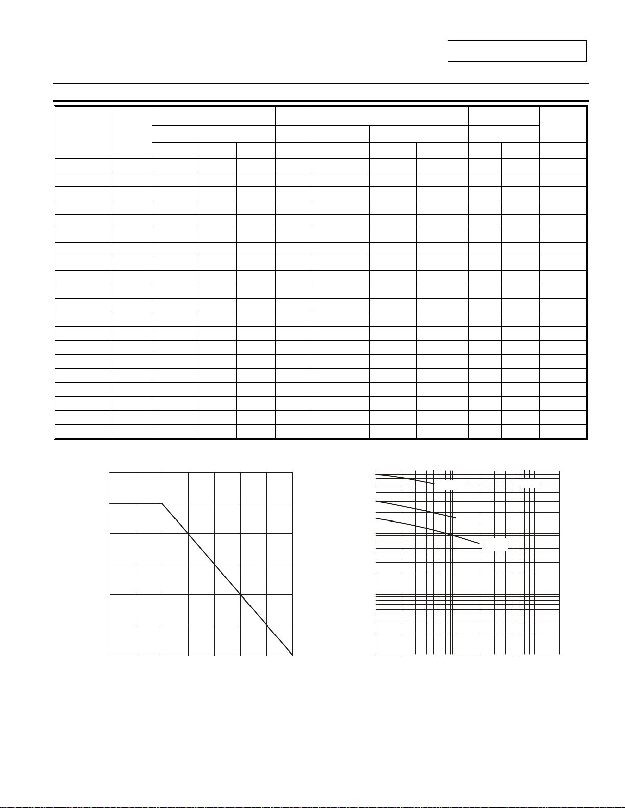
Electrical Characteristics @T
Zener Voltage
Type
Number
Marking
Code
Range (Note 4)
Nom (V) Min (V) Max (V) mA
= 25°C unless otherwise specified
A
Test
Current
V
IZT Z
Z @ IZT
Maximum Zener Impedance
Z
ZT @ IZT
ZK @ IZK
Ω Ω
Maximum
Reverse Current
I
R @ VR
mA µA V mA
SMAZ5V1 ZHK 5.1 4.84 5.40 100 5.0 500 1.0 2.5 1.0 196
SMAZ5V6 ZHL 5.60 5.32 5.88 100 2.0 250 2.0 5.0 2.0 179
SMAZ6V2 ZHN 6.20 5.89 6.51 100 2.0 200 2.0 5.0 3.0 161
SMAZ6V8 ZHO 6.80 6.46 7.14 100 2.0 200 1.0 5.0 4.0 147
SMAZ7V5 ZHQ 7.50 7.13 7.88 100 2.0 450 1.0 5.0 5.0 133
SMAZ8V2 ZHR 8.20 7.79 8.61 100 2.0 200 1.0 5.0 6.0 122
SMAZ9V1 ZHT 9.10 8.65 9.56 50 4.0 200 1.0 5.0 7.0 110
SMAZ10 ZHU 10.00 9.50 10.50 50 4.0 200 1.0 1.0 7.6 100
SMAZ12 ZHW 12.00 11.40 12.60 50 7.0 150 1.0 1.0 9.1 83
SMAZ15 ZHZ 15.00 14.25 15.75 50 10 150 1.0 1.0 11.4 67
SMAZ16 ZJA 16.00 15.20 16.80 25 15 150 1.0 0.5 12.2 63
SMAZ18 ZJF 18.00 17.10 18.90 25 15 150 1.0 0.5 13.7 56
SMAZ20 ZJG 20.00 19.00 21.00 25 15 180 1.0 0.5 15.2 50
SMAZ22 ZJK 22.00 20.90 23.10 25 15 180 1.0 0.5 16.7 45
SMAZ24 ZJL 24.00 22.80 25.20 25 15 180 1.0 0.5 18.2 42
SMAZ27 ZJN 27.00 25.65 28.35 25 15 200 1.0 0.5 20.5 37
SMAZ30 ZJQ 30.00 28.50 31.50 25 15 250 1.0 0.5 22.8 33
SMAZ33 ZJR 33.00 31.35 34.65 25 15 300 1.0 0.5 25.1 30
SMAZ36 ZJS 36.00 34.20 37.80 10 40 350 1.0 0.5 27.4 28
SMAZ39 ZJT 39.00 37.05 40.95 10 40 450 1.0 0.5 29.6 26
Notes: 4. Short duration pulse test used to minimize self-heating effect.
1.2
1,000
SMAZ5V6
f = 1MHz
I
ZM Max
(Note 3)
1.0
E (pF)
0.8
(W)
100
N
IT
SMAZ12
SMAZ27
0.6
EAK
pk
0.4
L
10
, TOT
T
0.2
0
0
50
T , AMBIENT TEMPERATURE ( C)
A
100
150
°
Fig. 1 Power D issipat i o n vs. Ambient Temperature
175
0
1 10 100 200
V , REVERSE VOLTAGE (V)
R
Fig. 2 Typical Total Capacitance vs. Rever se Vol t age
SMAZ5V1 - SMAZ39
Document number: DS18015 Rev. 16 - 2
2 of 5
www.diodes.com
June 2009
© Diodes Incorporated
Page 3

P
FORWARD CUR
R
N
T
SMAZ5V1 - SMAZ39
20
T = 25C
°
10
J
(A)
2,000
1,000
100
E
10
1
1
0.1
EAK
FM
I,
0.1
0 0.5 1.0 1.5 2.0 2.5
V , PEAK FORWARD VOLTAGE (V)
FM
Fig. 3 Peak Forward Current vs. Peak Forward Voltage
1,000
0.01
0.001
110100500
V , ZENER REGULATION VOLTAGE (V)
ZT
Fig. 4 Leakage Current vs. Regulation Voltage
I = 5.0mA
100
ZT
I = 10mA
ZT
10
I = 20mA
ZT
1
I = 100mA
ZT
0.1
110100500
V , ZENER REGULATION VOLTAGE (V)
ZT
Fig. 5 Differential Resistance vs. Regulation Voltage
Ordering Information (Note 5)
Device*
SMAZx-13-F
*x = Device Voltage, e.g., SMAZ5V1-13-F.
Notes: 5. For packaging details, go to our website at http://www.diodes.com/datasheets/ap02007.pdf.
Packaging Shipping
SMA 5000/Tape & Reel
Marking Information
YWW
xxx
SMAZ5V1 - SMAZ39
Document number: DS18015 Rev. 16 - 2
xxx = Product type marking code
(See Electric Characteristics Table)
= Manufacturers’ code marking
YWW = Date code marking
Y = Last digit of year (ex: 2 for 2002)
WW = Week code 01 to 52
3 of 5
www.diodes.com
June 2009
© Diodes Incorporated
Page 4

Package Outline Dimensions
B
A
J
H
G
E
Suggested Pad Layout
SMAZ5V1 - SMAZ39
SMA
Dim Min Max
C
D
A 2.29 2.92
B 4.00 4.60
C 1.27 1.63
D 0.15 0.31
E 4.80 5.59
G 0.05 0.20
H 0.76 1.52
J 2.01 2.30
All Dimensions in mm
Dimensions Value (in mm)
Z
G
X
Y 2.5
C
6.5
1.5
1.7
4.0
SMAZ5V1 - SMAZ39
Document number: DS18015 Rev. 16 - 2
4 of 5
www.diodes.com
June 2009
© Diodes Incorporated
Page 5

IMPORTANT NOTICE
DIODES INCORPORATED MAKES NO WARRANTY OF ANY KIND, EXPRESS OR IMPLIED, WITH REGARDS TO THIS DOCUMENT,
INCLUDING, BUT NOT LIMITED TO, THE IMPLIED WARRANTIES OF MERCHANTABILITY AND FITNESS FOR A PARTICULAR PURPOSE
(AND THEIR EQUIVALENTS UNDER THE LAWS OF ANY JURISDICTION).
Diodes Incorporated and its subsidiaries reserve the right to make modifications, enhancements, improvements, corrections or other changes
without further notice to this document and any product described herein. Diodes Incorporated does not assume any liability arising out of the
application or use of this document or any product described herein; neither does Diodes Incorporated convey any license under its patent or
trademark rights, nor the rights of others. Any Customer or user of this document or products described herein in such applications shall assume
all risks of such use and will agree to hold Diodes Incorporated and all the companies whose products are represented on Diodes Incorporated
website, harmless against all damages.
Diodes Incorporated does not warrant or accept any liability whatsoever in respect of any products purchased through unauthorized sales channel.
Should Customers purchase or use Diodes Incorporated products for any unintended or unauthorize d application, Customers shall indemnify and
hold Diodes Incorporated and its representatives harmless against all claims, damages, expenses, and attorney fees arising out of, directly or
indirectly, any claim of personal injury or death associated with such unintended or unauthorized application.
Products described herein may be covered by one or more United States, international or foreign patents pending. Product names and markings
noted herein may also be covered by one or more United States, international or foreign trademarks.
LIFE SUPPORT
Diodes Incorporated products are specifically not authorized for use as critical components in life support devices or systems without the express
written approval of the Chief Executive Officer of Diodes Incorporated. As used herein:
A. Life support devices or systems are devices or systems which:
1. are intended to implant into the body, or
2. support or sustain life and whose failure to perform when properly used in accordance with instructions for use provided in the
labeling can be reasonably expected to result in significant injury to the user.
B. A critical component is any component in a life support device or system whose failure to perform can be reasonably expected to cause the
failure of the life support device or to affect its safety or effectiveness.
Customers represent that they have all necessary expertise in the safety and regulatory ramifications of their life support devices or systems, and
acknowledge and agree that they are solely responsible for all legal, regulatory and safety-related requirements concerning their products and any
use of Diodes Incorporated products in such safety-critical, life support devices or systems, notwithstanding any devices- or systems-related
information or support that may be provided by Diodes Incorporated. Further, Customers must fully indemnify Diodes Incorporated and its
representatives against any damages arising out of the use of Diodes Incorporated products in such safety-critical, life support devices or systems.
Copyright © 2009, Diodes Incorporated
www.diodes.com
SMAZ5V1 - SMAZ39
SMAZ5V1 - SMAZ39
Document number: DS18015 Rev. 16 - 2
5 of 5
www.diodes.com
June 2009
© Diodes Incorporated
 Loading...