Diodes SM05 User Manual

p
θ
Features
• 300 Watts Peak Pulse Power (tp = 8x20μs)
• IEC 61000-4-2 (ESD): Air – 15kV, Contact – 8kV
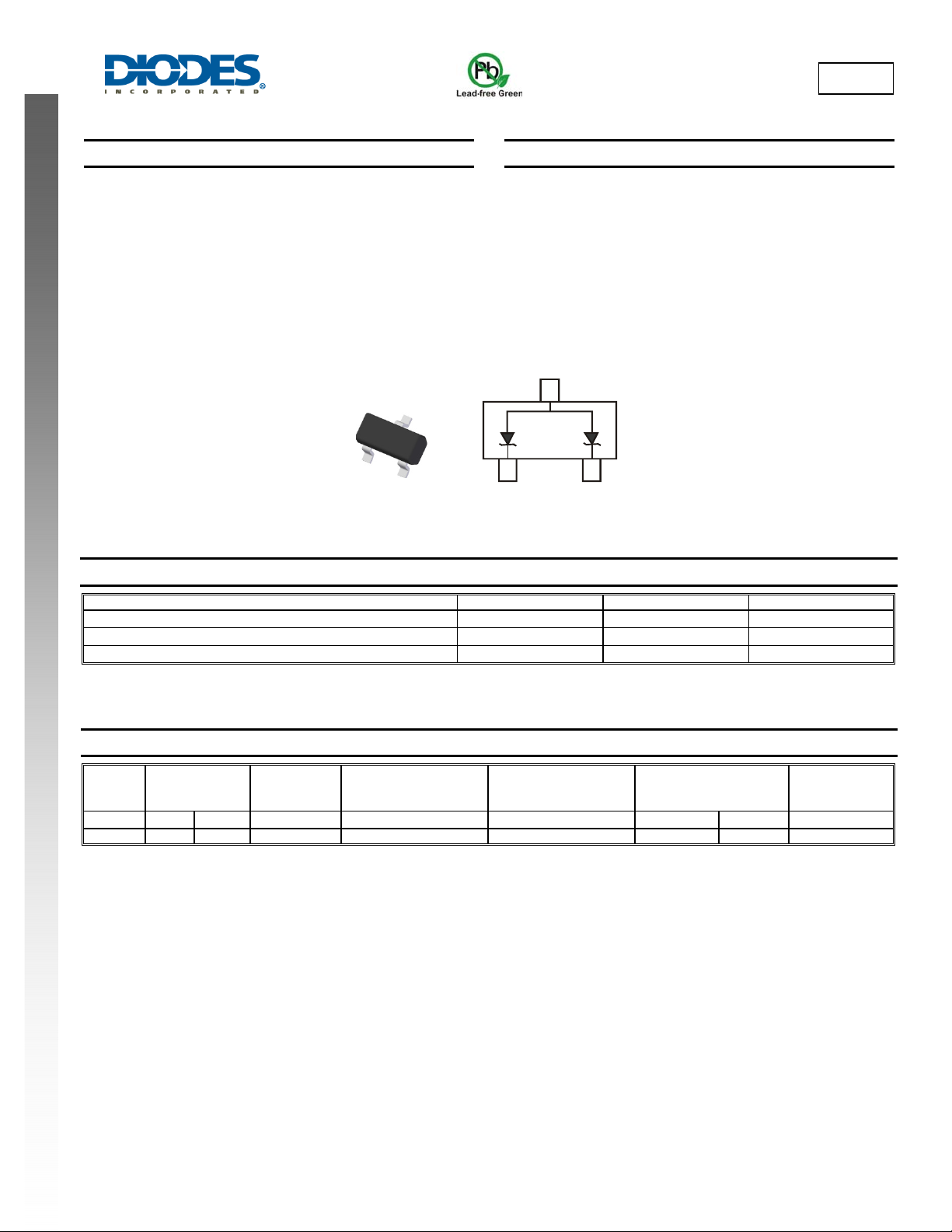
• Dual Common Anode TVS
• SOT-23 Package Allows Either Two Separate Unidirectional
Configurations or a Single Bidirectional Configuration
• Lead Free/RoHS Compliant (Note 3)
• “Green” Device (Note 4)
• Qualified to AEC-Q101 Standards for High Reliability
NEW PRODUCT
Top View
DUAL SURFACE MOUNT TVS
Mechanical Data
• Case: SOT-23
• Case Material: Molded Plastic, “Green” Molding Compound,
Note 3. UL Flammability Classification Rating 94V-0
• Moisture Sensitivity: Level 1 per J-STD-020
• Terminals: Matte Tin Finish annealed over Alloy 42 leadframe
(Lead Free Plating) Solderable per MIL-STD-202, Method 208
• Ordering Information: See Page 2
• Marking Information: See Page 2
• Weight: 0.0089 grams (approximate)
Device Schematic
SM05
Thermal Characteristics
Characteristic Symbol Value Unit
Peak Pulse Power (tp = 8x20μs) (Note 6) TA = 25°C P
Thermal Resistance, Junction to Ambient (Note 6) TA = 25°C
Operating and Storage Temperature Range
k
R
JA
, T
T
J
STG
Electrical Characteristics @T
Reverse
Standoff
Voltage
V
RWM
Breakdown
Voltage
V
Min (V) Max (V)
(V)
BR
@ IT
Test
Current
IT (mA) IR (μA) VC (V)
= 25°C unless otherwise specified (Note 7)
A
Max. Reverse
Leakage @ V
(Note 5)
RWM
Max. Clamping
Voltage @ I
(Note 2)
PP
= 5A
5 6.2 7.3 1.0 10 9.8 20.6 17 230
Notes: 1. VR = 0V, f = 1MHz.
2. Clamping voltage value is based on an 8x20 μs peak pulse current (I
3. No purposefully added lead.
4. Diodes Inc.’s “Green” policy can be found on our website at http://www.diodes.com/products/lead_free/index.php.
5. Short duration pulse test used to minimize self-heating effect.
6. Device mounted on FR-4 PC board with suggested pad layout, which can be found on our website at http://www.diodes.com/datasheets/ap02001.pdf.
Measured across pin 1 and pin 2.
) waveform.
pp
SM05
Document number: DS31828 Rev. 4 - 2
1 of 4
www.diodes.com
300 W
417
-55 to +150
Max. Clamping Voltage
@ I
V
V
(Note 2)
C
PP
(V) I
C
(A) (pF)
PP
°C/W
°C
Typical
Capacitance C
(Note 1)
April 2010
© Diodes Incorporated
T

P
P
U
RATING
O
P, P
P
U
P
OWER
C, TOT
CAPACITAN
C
NEW PRODUCT
SM05
100
F
75
IN %
50
LSE DE
25
PEAK POWER OR CURRENT
EAK
0
0 25 50 75 100 125 150 175 200
T , AMBIENT TEMPERATURE (°C)
A
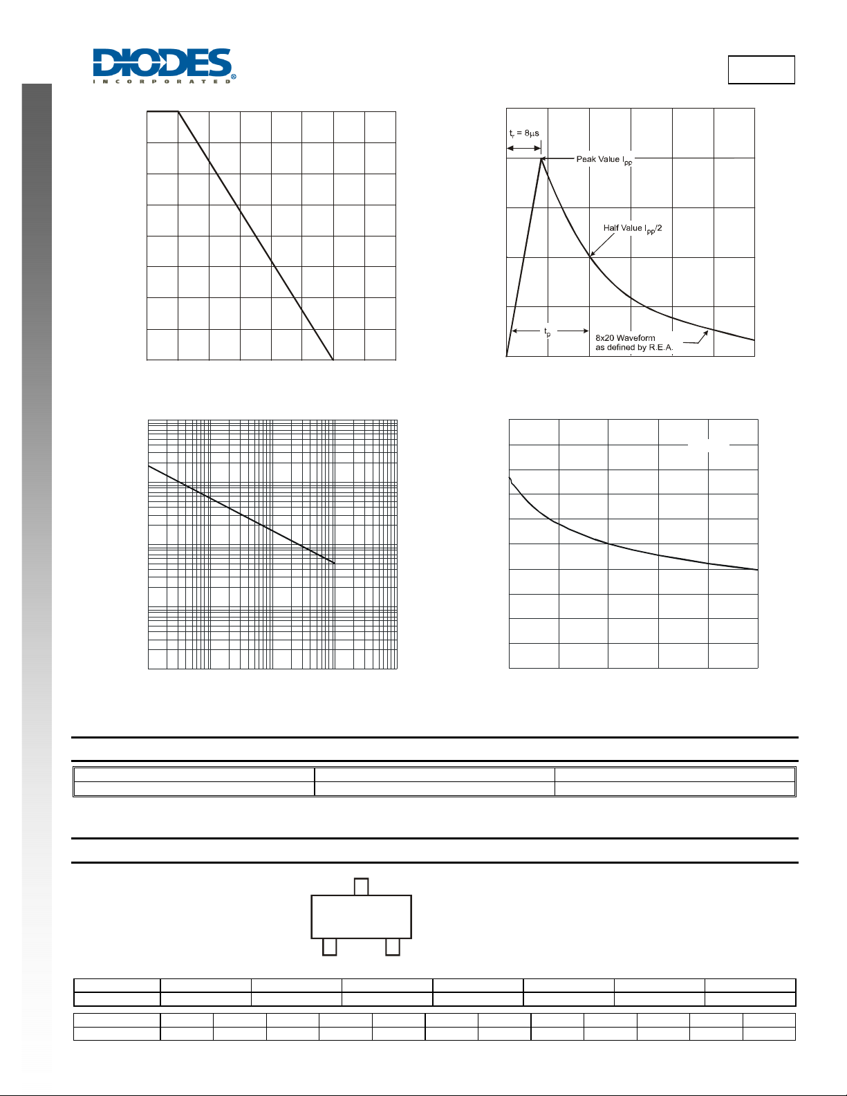
Fig. 1 Pulse Derating Curve
10,000
I , PEAK PULSE CURRENT (%I )
100
PppP
300
270
50
0
0
20 40
t, TIME ( s)
Fig. 2 Pulse Waveform
μ
f = 1MHz
60
1,000
(W)
100
LSE
EAK
10
PK
1
1 10 100 1,000 10,000
Fig. 3 Max. Peak Pulse Power vs. Pulse Duration
t , PULSE DURATION (µs)
d
240
210
E (pF)
180
150
120
AL
90
T
60
30
0
012 345
Fig. 4 Typical Total Capacitance vs. Reverse Voltage
V , REVERSE VOLTAGE (V)
R
Ordering Information (Note 8)
Part Number Case Packaging
SM05-7 SOT-23 3000/Tape & Reel
Notes: 8. For packaging details, go to our website at http://www.diodes.com/datasheets/ap02007.pdf.
Marking Information
TV1
Date Code Key
Year 2010 2011 2012 2013 2014 2015 2016
Code X Y Z A B C D
Month Jan Feb Mar Apr May Jun Jul Aug Sep Oct Nov Dec
Code 1 2 3 4 5 6 7 8 9 O N D
SM05
Document number: DS31828 Rev. 4 - 2
TV1 = Product Type Marking Code
YM = Date Code Marking
YM
Y = Year (ex: X = 2010)
M = Month (ex: 9 = September)
2 of 4
www.diodes.com
April 2010
© Diodes Incorporated
 Loading...