DIODES SDM40E20LS Datasheet

Features
TCUDORPWEN
· Very Low Forward Voltage Drop
· Guard Ring Construction for
Transient Protection
· High Conductance
Mechanical Data
· Case: SOT-23, Plastic
· Case material - UL Flammability Rating
Classification 94V-0
· Moisture sensitivity: Level 1 per J-STD-020A
· Polarity: See Diagram
· Leads: Solderable per MIL-STD-202,
Method 208
· Marking: Date Code and Type Code
· Type Code: KSW
Weight: 0.004 grams (approx.)
· Ordering Information: See Page 3
SDM40E20LS
DUAL SURFACE MOUNT SCHOTTKY BARRIER DIODE
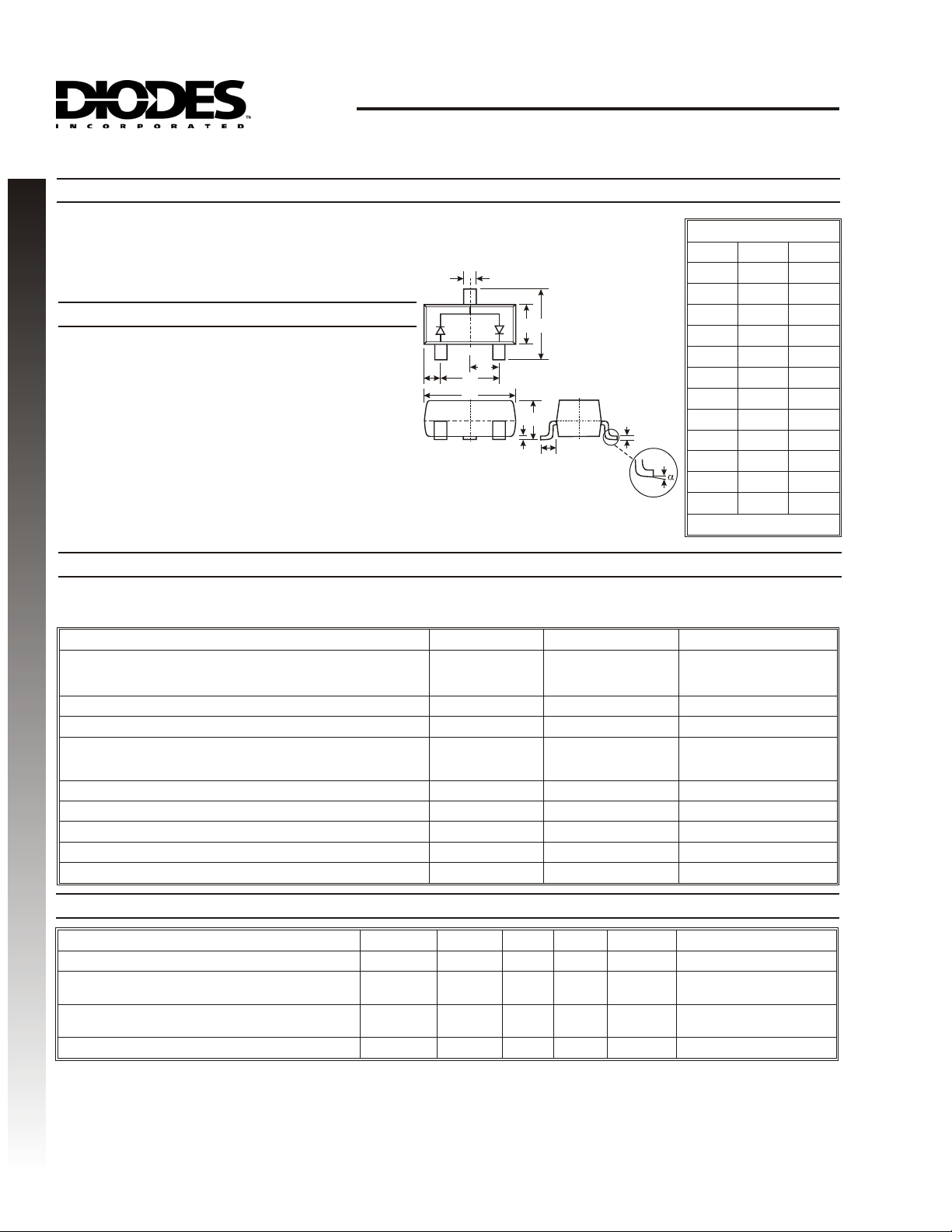
SOT-23
Dim Min Max
A
B
C
D
E
G
H
J
K
L
M
a
0.37 0.51
1.20 1.40
2.30 2.50
0.89 1.03
0.45 0.60
1.78 2.05
2.80 3.00
0.013 0.10
0.903 1.10
0.45 0.61
0.85 0.80
0° 8°
E
TOP VIEW
G
H
A
B
C
D
K
J
L
M
All Dimensions in mm
Maximum Ratings
Single phase, half wave, 60Hz, resistive or inductive load.
For capacitive load, derate current by 20%.
Peak Repetitive Reverse Voltage
Working Peak Reverse Voltage
DC Blocking Voltage
RMS Reverse Voltage
Forward Continuous Current (Note 1)
Non-Repetitive Peak Forward Surge Current
8.3ms single half sine-wave superimposed on rated load
(JEDEC Method)
Power Dissipation (Note 1)
Typical Thermal Resistance Junction to Ambient (Note 1)
Power Dissipation (Note 2)
Typical Thermal Resistance Junction to Ambient (Note 2)
Operating and Storage Temperature Range
Electrical Characteristics
Characteristic Symbol
Reverse Breakdown Voltage (Note 3)
Forward Voltage Drop (Note 3)
Leakage Current (Note 3)
Total Capacitance
Notes: 1. Device mounted on FR-5 1.0 x 0.75 x 0.062 inch PCB pad layout as shown on Diodes Inc. suggested pad layout AP02001,
which can be found on our website at http://www.diodes.com/datasheets/ap02001.pdf.
2. Device mounted on Alumina PCB, 0.4 inch x 0.3 inch x 0.024 inch; pad layout as shown on Diodes Inc. suggested pad layout
document AP02001, which can be found on our website at http://www.diodes.com/datasheets/ap02001.pdf.
3. Short duration test pulse used to minimize self-heating effect.
@ TA = 25°C unless otherwise specified
Characteristic Symbol
V
RRM
V
RWM
V
R
V
R(RMS)
I
FM
I
FSM
P
d
R
qJA
P
d
R
qJA
Tj,T
STG
@ TA = 25°C unless otherwise specified
Min Typ
V
(BR)R
V
F
I
R
C
T
20 ¾¾ V
¾
¾
¾
¾
¾ 170 ¾ pF
SDM40E20LS
20 V
14 V
0.4 A
2A
225 mW
444 °C/W
300 mW
333 °C/W
-55 to +125 °C
Max Unit Test Conditions
¾¾0.310
0.430
¾
¾
100
250
V
mA
Unit
IR = 0.5mA
I
= 0.1A
F
= 0.5A
I
F
V
= 10V
R
= 20V
V
R
f = 1MHz, V
= 0VDC
r
DS30298 Rev. 2 - 2 1 of 3 SDM40E20LS

TCUDORPWEN
O
10
1000
1000
RWARD CURRENT (A)
0.40
0.30
1.0
0.20
0.1
0.10
F(AV)
I , AVERAGE F
0
050100150
25 75 125
T , TERMINAL TEMPERATURE (°C)
T
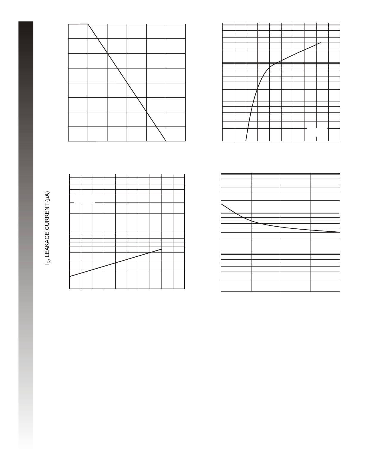
Fig. 1 Forward Current Derating Curve
T=25°C
j
F
I , INSTANTANEOUS FWD CURRENT (A)
0.01
0.20 0.4 0.6 0.8 1.0
V , INSTANTANEOUS FORWARD VOLTAGE (V)
F
Fig.2 Typical Forward Characteristics
T=25°C
j
100
100
10
T
C , CAPACITANCE (pF)
10
0
5
V , REVERSE VOLTAGE (V)
10 15
R
Fig.3 Typical Reverse Characteristics
20
25
1.0
0 5 10 15 20
V , REVERSE VOLTAGE (V)
R
Fig.4 Typ. Total Capacitance vs Reverse Voltage
DS30298 Rev. 2 - 2 2 of 3 SDM40E20LS
 Loading...