Diodes SDM1L30CSP User Manual

Product Summary
(V)
V
V
(V) IO (A)
RRM
30 1.0 0.40 1.0
F(MAX)
@ +25°C
I
R(MAX)
@ +25°C
Description and Applications
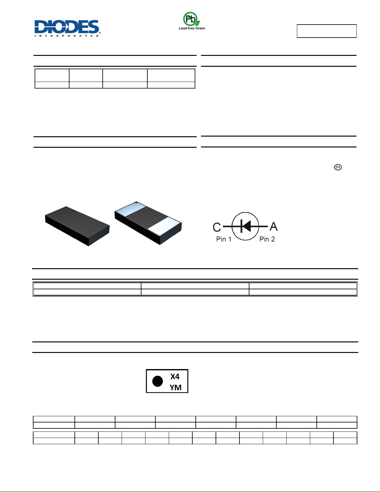
The SDM1L30CSP is a 30-volt 1A Schottky barrier diode that is
NEW PRODUCT
optimized for low forward voltage and soft switching characteristics to
meet the needs of wireless charging applications. It is housed in a
compact chip scale package (CSP) that occupies only 2 mm
space. It is ideally suited for use in portable applications.
NEW PRODUCT
SDM1L30CSP
1A SCHOTTKY BARRIER DIODE CHIP SCALE PACKAGE
(mA)
Features and Benefits
2 mm2 Footprint – 67% smaller than PowerDI123
Off Board Profile of 0.3mm – 70% thinner than PowerDI123
Low Forward Voltage Drop reduces Power Dissipation
Soft switching characteristic ensures that EMI and EFI are
minimised
Guard Ring Die Construction for Transient Protection
Totally Lead-Free & Fully RoHS Compliant (Notes 1 & 2)
Halogen and Antimony Free. “Green” Device (Note 3)
Mechanical Data
Case: X2-WLB2010-2
Moisture Sensitivity: Level 1 per J-STD-020
2
board-
Terminals: Solderable per MIL-STD-202, Method 208
Polarity: Cathode Dot
Weight: 0.15mg
Ordering Information
Part Number Case Packaging
SDM1L30CSP-7 X2-WLB2010-2 3,000/Tape & Reel
Notes: 1. No purposely added lead. Fully EU Directive 2002/95/EC (RoHS) & 2011/65/EU (RoHS 2) compliant.
2. See http://www.diodes.com/quality/lead_free.html for more information about Diodes Incorporated’s definitions of Halogen- and Antimony-free, "Green"
and Lead-free.
3. Halogen- and Antimony-free "Green” products are defined as those which contain <900ppm bromine, <900ppm chlorine (<1500ppm total Br + Cl) and
<1000ppm antimony compounds.
4. For packaging details, go to our website at http://www.diodes.com/products/packages.html.
(Note 4)
Marking Information
Date Code Key
Year 2014 2015 2016 2017 2018 2019 2020
Code B C D E F G H
Month Jan Feb Mar Apr May Jun Jul Aug Sep Oct Nov Dec
Code 1 2 3 4 5 6 7 8 9 O N D
SDM1L30CSP
Document number: DS35649 Rev. 5 - 2
1 of 5
www.diodes.com
X4 = Product Type Marking Code
YM = Date Code Marking
Y = Year (ex: B = 2014)
M = Month (ex: 9 = September)
Dot denotes Cathode Pin
March 2014
© Diodes Incorporated

Maximum Ratings (@T
Single phase, half wave, 60Hz, resistive or inductive load.
For capacitance load, derate current by 20%.
Peak Repetitive Reverse Voltage
Average Rectified Output Current
Non-Repetitive Peak Forward Surge Current 8.3ms
Single Half Sine-Wave Superimposed on Rated Load
= +25°C, unless otherwise specified.)
A
Characteristic Symbol Value Unit
Thermal Characteristics
Characteristic Symbol Value Unit
NEW PRODUCT
Typical Thermal Resistance Junction to Ambient (Note 5)
Operating and Storage Temperature Range
NEW PRODUCT
Electrical Characteristics (@T
V
R
θJA
T
, T
J
STG
= +25°C, unless otherwise specified.)
A
I
FSM
RRM
I
O
SDM1L30CSP
30 V
1.0 A
25 A
130 °C/W
-55 to +150 °C
Characteristic Symbol Min Typ Max Unit Test Condition
Forward Voltage Drop
Leakage Current (Note 6)
Total Capacitance CT — 150 — pF VR = 5V, f = 1.0 MHz
Notes: 5. Device mounted on FR-4 substrate PC board, with minimum recommended pad layout per http://www.diodes.com/datsheets/ap02001.pdf.
6. Short duration pulse test used to minimize self-heating effect.
V
F
I
R
SDM1L30CSP
Document number: DS35649 Rev. 5 - 2
— 0.35
— 0.29
— 0.47 1.0 mA
— 17 — mA
2 of 5
www.diodes.com
0.40
—
I
= 1.0A, TJ = +25°C
V
F
I
= 1.0A, TJ = +85°C
F
V
= 30V, TJ = +25°C
R
V
= 30V, TJ = +85°C
R
© Diodes Incorporated
March 2014
 Loading...