Diodes SDM03U40 User Manual

)
θ
(BR)
Please click here to visit our online spice models database.
Features
• Low Forward Voltage Drop
• Guard Ring Die Construction for Transient Protection
• Ideal for low logic level applications
• Low Capacitance
• Lead Free by Design/RoHS Compliant (Note 1)
• "Green" Device, Note 4 and 5
• Qualified to AEC-Q101 Standards for High Reliability
Maximum Ratings @T
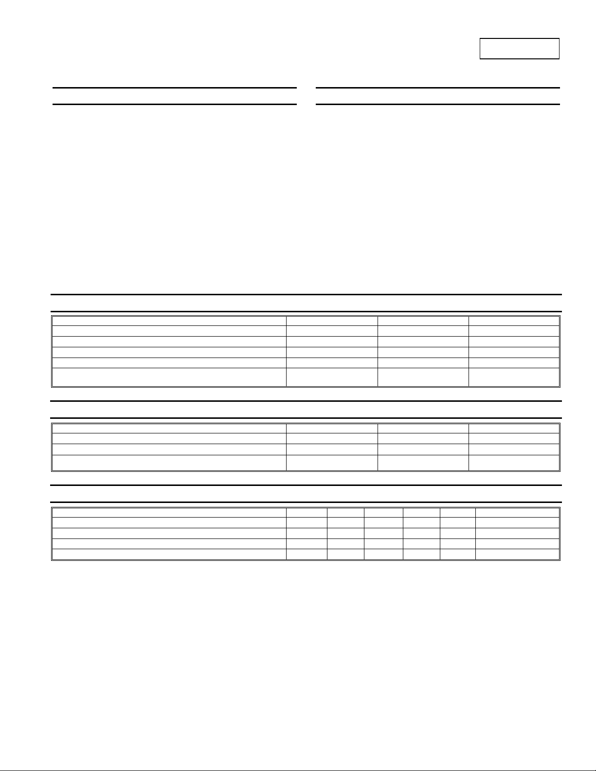
Characteristic Symbol Value Unit
Peak Reverse Voltage
DC Reverse Voltage
RMS Reverse Voltage
Average Rectified Current
Non-Repetitive Peak Forward Surge Current @8.3ms
Single half sine-wave superimposed on rated load
= 25°C unless otherwise specified
A
SDM03U40
SURFACE MOUNT SCHOTTKY BARRIER DIODE
Mechanical Data
• Case: SOD-523
• Case Material: Molded Plastic, "Green" Molding Compound,
Note 5. UL Flammability Classification Rating 94V-0
• Moisture Sensitivity: Level 1 per J-STD-020D
• Terminal Connections: Cathode Band
• Terminals: Finish - Matte Tin annealed over Alloy 42 leadframe.
Solderable per MIL-STD-202, Method 208
• Marking Information: See Page 3
• Ordering Information: See Page 3
• Weight: 0.002 grams (approximate)
Top View
40 V
30 V
21 V
30 mA
200 mA
V
R(RMS
VRM
VR
IO
I
FSM
Thermal Characteristics
Characteristic Symbol Value Unit
Power Dissipation (Note 2)
Thermal Resistance, Junction to Ambient (Note 2)
Operating and Storage Temperature Range
Electrical Characteristics @T
Reverse Breakdown Voltage (Note 3)
Forward Voltage
Peak Reverse Current (Note 3)
Total Capacitance
Notes: 1. No purposefully added lead.
code 0627 are built with Non-Green Molding Compound and may contain Halogens or Sb2O3 Fire Retardants.
2. Part mounted on FR-4 board with recommended pad layout, which can be found on our website at http://www.diodes.com/datasheets/ap02001.pdf.
3. Short duration pulse test used to minimize self-heating effect.
4. Diodes Inc.'s "Green" Policy can be found on our website at http://www.diodes.com/products/lead_free/index.php.
5. Product manufactured with date code 0627 (week 27, 2006) and newer are built with Green Molding Compound. Product manufactured prior to date
SDM03U40
Document number: DS30392 Rev. 9 - 2
Characteristic Symbol Min Typ Max Unit Test Conditions
A
PD
R
T
J, TSTG
= 25°C unless otherwise specified
V
R
VF
IR
CT
1 of 3
www.diodes.com
JA
40
⎯
⎯ ⎯
⎯
150 mW
667
-40 to +125
⎯ ⎯
290 370 mV
0.5
2
⎯
V
μA
pF
°C/W
°C
I
uA
R = 10
IF = 1mA
VR = 30V
VR = 1V, f = 1.0 MHz
January 2009
© Diodes Incorporated

TANT
O
US FORWARD CUR
RENT
TANT
O
US R
R
CUR
RENT
C, TOT
CAPACITAN
C
F
R
R
REC
OVER
Y T
P
P
O
R
PAT
O
SDM03U40
1
(A)
(A)
100m
10m
1m
SE
EVE
100n
ANE
ANE
10n
F
I , INS
100
)
0
0.2 0.4 0.6
V , INSTANTANEOUS FORWARD VOL TAGE (V)
F
0.8 1.0
1.2
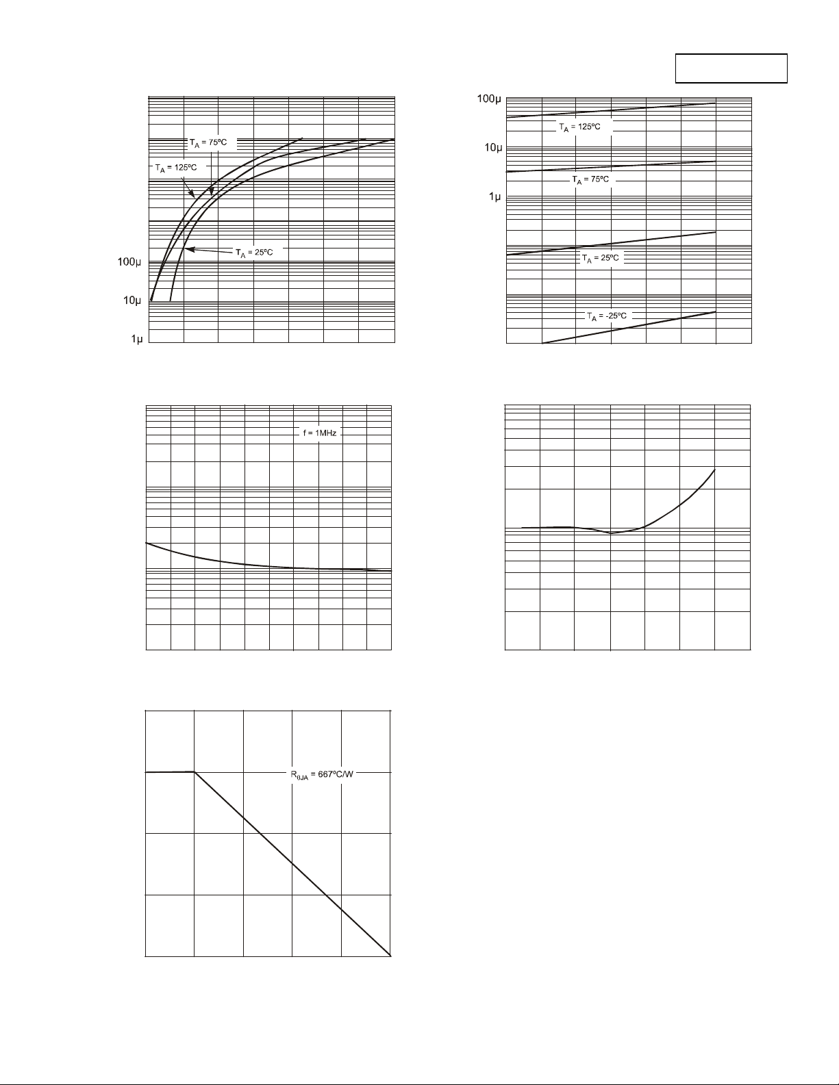
Fig. 1 Typical Forward Characteristics
1.4
I, INS
R
1n
0
51015
V , INSTANTANEOUS REVERSE VOLTAGE (V)
R
20
Fig. 2 Typical Reverse Characteristics
10
5
25 30
35
E (p
AL
N (mW)
I
DISSI
T
200
150
100
10
1
0.1
0
5
V , DC REVERSE VOLT AGE (V)
10 15
R
Fig. 3 Total Capacitance vs . Reverse Volt age
20
25
IME (ns)
2
1
0.5
SE
EVE
0.2
rr
t,
0.1
0
48
I , FORWARD CURRENT (mA)
F
12 16 20
Fig. 4 Typical Reverse Recovery Time Characteristics
24
28
WE
50
,
D
0
025
T , AMBIENT TEMPERATURE ( C)
A
50
75 100
125
°
Fig. 5 Power Derating Curve
SDM03U40
Document number: DS30392 Rev. 9 - 2
2 of 3
www.diodes.com
January 2009
© Diodes Incorporated
 Loading...