

Page 1
)
A
Product Summary
V
(V) IO (mA) V
RRM
30 200 0.50 0.05
(V) @ +25°C I
F(MAX)
R(MAX
(mA) @ +25°C
Description
The SDM0230CSP is a 30-volt 0.2A schottky barrier diode that is
optimized for low forward voltage drop and low leakage current housed in
a compact chip scale package (CSP) that occupies only 0.18mm
space. The low thermal resistance enables designers to meet design
challenges of increasing efficiency whilst at the same time reducing
board space. It is ideally suited for use in portable applications.
NEW PRODUCT
Applications
Blocking Diode
Switching Diode
NEW PRODUCT
Reverse Protection Diode
Boost Diode
SDM0230CSP
0.2A SCHOTTKY BARRIER DIODE CHIP SCALE PACKAGE
Features and Benefits
0.18mm2 footprint – 70% smaller than DFN1006/SOD923
Off board profile of 0.3mm – more than 30% thinner than the
DFN1006
Low forward voltage of 0.50V (max) – minimises power
dissipation losses
Low leakage – maximises battery power
2
board-
Soft, Fast Switching Capability
Totally Lead-Free & Fully RoHS Compliant (Notes 1 & 2)
Halogen and Antimony Free. “Green” Device (Note 3)
Mechanical Data
Case: X3-WLCUS0603-3
Moisture Sensitivity: Level 1 per J-STD-020
Terminal Connections: Cathode Dot
Weight: 0.119mg
C
Pin 1
Pin 2
Ordering Information (Note 4)
Part Number Case Packaging
SDM0230CSP-7 X3-WLCUS0603-3 3,000/Tape & Reel
Notes: 1. No purposely added lead. Fully EU Directive 2002/95/EC (RoHS) & 2011/65/EU (RoHS 2) compliant.
2. See http://www.diodes.com/quality/lead_free.html for more information about Diodes Incorporated’s definitions of Halogen- and Antimony-free, "Green"
and Lead-free.
3. Halogen- and Antimony-free "Green” products are defined as those which contain <900ppm bromine, <900ppm chlorine (<1500ppm total Br + Cl) and
<1000ppm antimony compounds.
4. For packaging details, go to our website at http://www.diodes.com/products/packages.html.
Marking Information
X7 = Product Type Marking Code
Dot denotes Cathode Pin
SDM0230CSP
Document number: DS35649 Rev. 7 - 2
1 of 4
www.diodes.com
May 2013
© Diodes Incorporated
Page 2
T
T
O
U
FOR
R
C
U
R
R
T
N
TAN
TANEO
US R
R
CUR
REN
T
Maximum Ratings (@T
= +25°C, unless otherwise specified.)
A
Single phase, half wave, 60Hz, resistive or inductive load.
For capacitance load, derate current by 20%.
Characteristic Symbol Value Unit
Peak Repetitive Reverse Voltage
Average Rectified Output Current
Non-Repetitive Peak Forward Surge Current 8.3ms
Single Half Sine-Wave Superimposed on Rated Load
Thermal Characteristics
Characteristic Symbol Value Unit
NEW PRODUCT
Typical Thermal Resistance Junction to Ambient (Note 5)
Operating and Storage Temperature Range
NEW PRODUCT
Electrical Characteristics (@T
V
R
θJA
T
, T
J
STG
= +25°C, unless otherwise specified.)
A
I
FSM
RRM
I
O
SDM0230CSP
30 V
0.2 A
4.5 A
261 °C/W
-55 to +150 °C
Characteristic Symbol Min Typ Max Unit Test Condition
— 0.30
Forward Voltage Drop
V
F
— 0.42
— 0.36
Leakage Current (Note 6)
Junction Capacitance
Notes: 5. Device mounted on FR-4 substrate PC board, with minimum recommended pad layout per http://www.diodes.com/datsheets/ap02001.pdf.
6. Short duration pulse test used to minimize self-heating effect.
I
R
C
J
— — 50 µA
— 1.5 — mA
— 9 — pF
0.35
0.50
—
I
= 10mA, TJ = +25°C
F
V
I
= 200mA, TJ = +25°C
F
I
= 200mA, TJ = +125°C
F
V
= 30V, TJ = +25°C
R
V
= 30V, TJ = +125°C
R
VR = 15V, TJ = +25°C , f = 1MHz
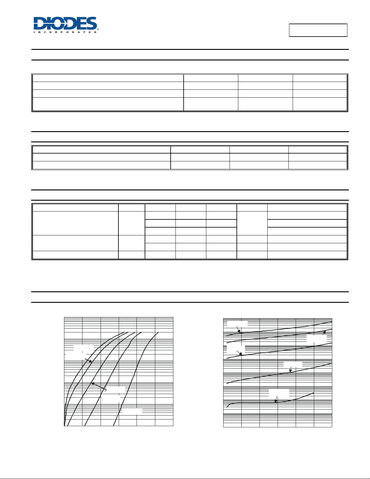
Typical Electrical Characteristics
1,000
(mA)
EN
100
T = 150°C
A
10
T = 125°C
A
D
WA
S
1
T = 85°C
A
T = 25°C
ANE
0.1
AN
0.01
F
I, INS
0 0.1 0.2 0.3 0.4 0.5 0.6
V , INSTANTANEOUS FORWARD VOLTAGE (V)
F
Figure 1 Typical Forward Characteristics
SDM0230CSP
Document number: DS35649 Rev. 7 - 2
A
T = -55°C
A
2 of 4
www.diodes.com
10000
(µA)
SE
EVE
S
R
I, I
0.0001
T = 150°C
A
1000
100
T = 85°C
A
10
T = 25°C
A
1
0.1
T = -55°C
0.01
A
0.001
0
5 1015202530
V , INSTANTANEOUS REVERSE VOLTAGE (V)
R
Figure 2 Typical Reverse Characteristics
T = 125°C
A
May 2013
© Diodes Incorporated
Page 3

C, TOT
CAP
C
TAN
C
SDM0230CSP
100
f=1MHz
E (pF)
I
10
A
AL
T
NEW PRODUCT
1
0 5 10 15 20 25 30
V , DC REVERSE VOLTAGE (V)
R
Figure 3 Total Capacitance vs. Reverse Voltage
NEW PRODUCT
Package Outline Dimensions
Please see AP02002 at http://www.diodes.com/datasheets/ap02002.pdf for latest version.
Cathode
Dot
D
L
︵3
X
E
e
1
b
︶
Cathode
e
X3-WLCUS0603-3
Dim Min Max Typ
A 0.24 0.30 —
A1 0.00 0.01 —
b 0.23 0.29 0.26
Anode
b1 0.075 0.135 0.105
D 0.290 0.300 0.295
b1 ︵2
X
︶
E 0.590 0.600 0.595
e — — 0.40
e1 — — 0.155
L 0.13 0.19 0.16
A
1
A
All Dimensions in mm
Seating Plane
Suggested Pad Layout
Please see AP02001 at http://www.diodes.com/datasheets/ap02001.pdf for the latest version.
Y
1
X
SDM0230CSP
Document number: DS35649 Rev. 7 - 2
Y
Y
www.diodes.com
3 of 4
Dimensions
X 0.30
Y 0.21
Y1 0.60
Value
(in mm)
May 2013
© Diodes Incorporated
Page 4

DIODES INCORPORATED MAKES NO WARRANTY OF ANY KIND, EXPRESS OR IMPLIED, WITH REGARDS TO THIS DOCUMENT,
INCLUDING, BUT NOT LIMITED TO, THE IMPLIED WARRANTIES OF MERCHANTABILITY AND FITNESS FOR A PARTICULAR PURPOSE
(AND THEIR EQUIVALENTS UNDER THE LAWS OF ANY JURISDICTION).
Diodes Incorporated and its subsidiaries reserve the right to make modifications, enhancements, improvements, corrections or other changes
without further notice to this document and any product described herein. Diodes Incorporated does not assume any liability arising out of the
application or use of this document or any product described herein; neither does Diodes Incorporated convey any license under its patent or
trademark rights, nor the rights of others. Any Customer or user of this document or products described herein in such applications shall assume
all risks of such use and will agree to hold Diodes Incorporated and all the companies whose products are represented on Diodes Incorporated
website, harmless against all damages.
Diodes Incorporated does not warrant or accept any liability whatsoever in respect of any products purchased through unauthorized sales channel.
Should Customers purchase or use Diodes Incorporated products for any unintended or unauthorized application, Customers shall indemnify and
hold Diodes Incorporated and its representatives harmless against all claims, damages, expenses, and attorney fees arising out of, directly or
indirectly, any claim of personal injury or death associated with such unintended or unauthorized application.
Products described herein may be covered by one or more United States, international or foreign patents pending. Product names and markings
NEW PRODUCT
noted herein may also be covered by one or more United States, international or foreign trademarks.
This document is written in English but may be translated into multiple languages for reference. Only the English version of this document is the
final and determinative format released by Diodes Incorporated.
NEW PRODUCT
Diodes Incorporated products are specifically not authorized for use as critical components in life support devices or systems without the express
written approval of the Chief Executive Officer of Diodes Incorporated. As used herein:
A. Life support devices or systems are devices or systems which:
1. are intended to implant into the body, or
labeling can be reasonably expected to result in significant injury to the user.
B. A critical component is any component in a life support device or system whose failure to perform can be reasonably expected to cause the
failure of the life support device or to affect its safety or effectiveness.
Customers represent that they have all necessary expertise in the safety and regulatory ramifications of their life support devices or systems, and
acknowledge and agree that they are solely responsible for all legal, regulatory and safety-related requirements concerning their products and any
use of Diodes Incorporated products in such safety-critical, life support devices or systems, notwithstanding any devices- or systems-related
information or support that may be provided by Diodes Incorporated. Further, Customers must fully indemnify Diodes Incorporated and its
representatives against any damages arising out of the use of Diodes Incorporated products in such safety-critical, life support devices or systems.
Copyright © 2013, Diodes Incorporated
www.diodes.com
2. support or sustain life and whose failure to perform when properly used in accordance with instructions for use provided in the
IMPORTANT NOTICE
LIFE SUPPORT
SDM0230CSP
SDM0230CSP
Document number: DS35649 Rev. 7 - 2
4 of 4
www.diodes.com
May 2013
© Diodes Incorporated
 Loading...