Please click here to visit our online spice models database.
General Description
• SDBN500B01 is best suited for switching inductive loads
in power switching applications. It improves efficiency
and reliability of power switching systems and it can
support continuous maximum current of 500 mA. It
features NPN transistor with high breakdown voltage
and discrete switching diode with high forward surge
NEW PRODUCT
current. It reduces component count, consumes less
space and minimizes parasitic losses. The component
devices can be used as a part of a circuit or as a stand
alone discrete device.
Features
• NPN Transistor with High Break-Down Voltage
• Switching Diode with High Forward Surge
• Low Switching and Conduction Losses
• Surface Mount Package Suited for Automated Assembly
• Lead Free By Design/RoHS Compliant (Note 1)
• "Green" Device (Note 2)
Mechanical Data
• Case: SOT-363
• Case Material: Molded Plastic, "Green" Molding
Compound. UL Flammability Classification Rating 94V-0
• Moisture Sensitivity: Level 1 per J-STD-020C
• Terminal Connections: See Figure
• Terminals: Finish ⎯ Matte Tin annealed over Alloy 42
leadframe. Solderable per MIL-STD-202, Method 208
• Marking and Type Code Information: See Page 6
• Ordering Information: See Page 6
• Weight: 0.016 grams (approximate)
SDBN500B01
500mA NPN TRANSISTOR SWITCH WITH SNUBBER DIODE
6
5
4
1
2
3
SOT-363
BQ1
5
2
NC
EQ1
4
Q1
3
CQ1
CD1
6
D1
1
AD1
Schematic and Pin Configuration
Sub-Component P/N Reference Device Type
MMBTA06_DIE Q1 NPN Transistor
BAS31_DIE D1 Switching Diode
Maximum Ratings: Total Device @T
Characteristic Symbol Value Unit
Power Dissipation (Note 3)
Power Derating Factor above 25°C
Output Current
= 25°C unless otherwise specified
A
P
d
P
der
I
out
200 mW
1.6
500 mA
mW / °C
Thermal Characteristics
Characteristic Symbol Value Unit
Junction Operating and Storage Temperature Range
Thermal Resistance, Junction to Ambient Air (Note 3)
(Equivalent to One Heated Junction of NPN Transistor)
Notes: 1. No purposefully added lead.
2. Diodes Inc.'s "Green" policy can be found on our website at http://www.diodes.com/products/lead_free/index.php.
3. Device mounted on FR-4 PCB, 1" x 0.85" x 0.062"; pad layout as shown on Diodes Inc. suggested pad layout document AP02001, which
can be found on our website at http://www.diodes.com/datasheets/ap02001.pdf.
Tj, T
R
θ
STG
JA
-55 to +150
625
°C
°C/W
DS30835 Rev. 3 - 2 1 of 6
www.diodes.com
SDBN500B01
© Diodes Incorporated

Maximum Ratings:
Sub-Component Device – Switching Diode (D1) @T
= 25°C unless otherwise specified
A
Characteristic Symbol Value Unit
Non-Repetitive Peak Reverse Voltage
Peak Repetitive Reverse Voltage
Working Peak Reverse Voltage
DC Blocking Voltage
RMS Reverse Voltage
Forward Continuous Current (Page 1: Note 3)
Average Rectified Output Current (Page 1: Note 3)
NEW PRODUCT
Non-Repetitive Peak Forward Surge Current @ t = 1.0 us 4 A
@ t = 1.0 s
V
V
V
V
R(RMS)
I
I
FSM
RM
RRM
RWM
V
R
FM
I
O
Sub Component Device - Discrete NPN Transistor (Q1) @T
100 V
75 V
53 V
500 mA
250 mA
2 A
= 25°C unless otherwise specified
A
Characteristic Symbol Value Unit
Collector-Base Voltage
Collector-Emitter Voltage
Emitter-Base Voltage
Output Current - continuous (Page 1: Note 3)
V
CBO
V
CEO
V
EBO
I
C
80 V
80 V
4 V
500 mA
Electrical Characteristics:
Switching Diode (D1) @T
Characteristic Symbol Min Typ Max Unit Test Condition
Reverse Breakdown Voltage (Note 4)
Forward Voltage Drop (Note 4)
Reverse Current (Note 4)
Total Capacitance
Reverse Recovery Time
Notes: 4. Short duration pulse test used to minimize self-heating effect.
= 25°C unless otherwise specified
A
V
(BR)R
75
0.62
V
FM
⎯ ⎯
⎯ ⎯
⎯ ⎯
⎯ ⎯
I
R
⎯ ⎯
⎯ ⎯
⎯ ⎯
C
T
t
rr
⎯ ⎯
⎯ ⎯
⎯
⎯
⎯
0.37
0.855
1
1.25
2.5
50
30
25
4 pF
4 ns
V
IR = 10 μA
IF = 5 mA
IF = 10 mA
V
IF = 100 mA
IF = 150 mA
VR = 75V
VR = 75V, Tj = 150 °C
μA
VR = 25V, Tj = 150 °C
VR = 20V
VR = 0V, f = 1.0 MHz
IF = IR = 10mA, Irr = 0.1xIR, RL = 100 Ω
NEW PRODUCT
DS30835 Rev. 3 - 2 2 of 6
www.diodes.com
SDBN500B01
© Diodes Incorporated

P, P
OWER
P
T
O
N
Discrete NPN Transistor (Q1) @T
OFF CHARACTERISTICS (Note 4)
Collector-Base Breakdown Voltage
Collector-Emitter Breakdown Voltage
Emitter-Base Breakdown Voltage
Collector Cutoff Current
Base Cutoff Current (I
Collector-Base Cut Off Current
Collector-Emitter Cut Off Current, I
NEW PRODUCT
Emitter-Base Cut Off Current
ON CHARACTERISTICS (Note 4)
DC Current Gain
Collector-Emitter Saturation Voltage
Base-Emitter Turn-on Voltage
Base-Emitter Saturation Voltage
SMALL SIGNAL CHARACTERISTICS
Output Capacitance
Input Capacitance
Current Gain-Bandwidth Product
SWITCHING CHARACTERISTICS
Delay Time
Rise Time
Pulse Test: Pulse width, tp<300uS, Duty Cycle, d<=2%
Notes: 4. Short duration pulse test used to minimize self-heating effect.
Characteristic Symbol Min Max Unit Test Condition
V
V
V
) I
BEX
O(OFF)
V
= 25°C unless otherwise specified
A
BR(CBO)
BR(CEO)
(BR)EBO
I
CEX
BL
I
CBO
I
CEO
I
EBO
80
80
4
⎯
⎯
⎯
⎯
⎯
100 nA
100 nA
100 nA
100 nA
100 nA
60
80
h
FE
100
100
90
80
0.1 V
0.25 V
0.35 V
0.98 V
0.95 V
1.2 V
CE(SAT)
V
BE(ON)
V
BE(SAT)
C
OBO
C
IBO
f
T
t
d
t
⎯
⎯
⎯
⎯
⎯
⎯
⎯
⎯
100
⎯
r
⎯
⎯
⎯
⎯
V
V
V
IC = 10 μA, IE = 0
IC = 1.0 mA, IB = 0
IE = 100 μA, IC = 0
VCE = 60V, V
VCE = 60V, V
EB(OFF)
EB(OFF)
= 3.0V
= 3.0V
VCB = 80V, IE = 0
VCE = 80V, IB = 0
VEB = 5V, IC = 0
⎯ ⎯ V
⎯ ⎯ V
⎯ ⎯ V
⎯ ⎯ V
= 1V, IC = 100 μA
CE
= 1V, IC = 1 mA
CE
= 1V, IC = 10 mA
CE
= 1V, IC = 50 mA
CE
⎯ ⎯ VCE = 1V, IC = 100 mA
⎯ ⎯ V
= 1V, IC = 200 mA
CE
IC = 10 mA, IB = 1 mA
IC = 100 mA, IB = 10 mA
IC = 200 mA, IB = 20 mA
VCE = 5V, IC = 2 mA
IC = 10 mA, IB = 1 mA
IC = 100 mA, VCE = 1V
4 pF
6 pF
⎯
MHz
35 ns
35 ns
VCB = 5.0 V, f = 1.0MHz, IE = 0
VEB = 5.0 V, f = 1.0MHz, IC = 0
V
= 2 V, IC = 10mA, f = 100MHz
CE
VCC = 3.0 V, IC = 10mA,
= 0.5V, IB1 = 1.0mA
V
BE(OFF)
Typical Characteristics
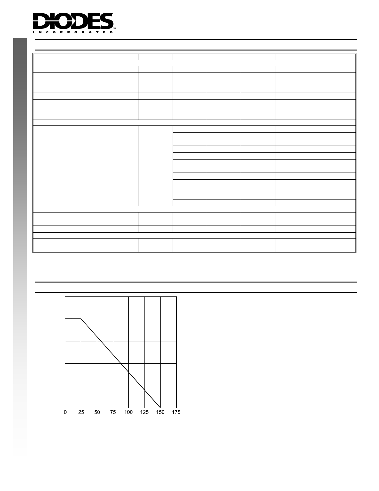
250
200
(mW)
I
150
A
DISSI
D
100
50
R = 625°C/W
θ
JA
0
T , AMBIENT TEMPERATURE (°C)
A
Fig. 1, Maximum Power Dissipation vs.
Ambient T emperature
DS30835 Rev. 3 - 2 3 of 6
www.diodes.com
SDBN500B01
© Diodes Incorporated
 Loading...